PREFACE
The MOS Technology, Inc. MGS6500 Microcomputer System offering combines the best features of second generation families into a product line that is both a price and performance leader. A growing array of products and a unique micro- processor family provide the customer with answers to the complex design prob- lems confronting today's programmers and designers. Integrated circuit fabrication techniques have moved microprocessors to the forefront of complex, sophisticated components. The MCS6500 family benefits from an advanced but proven process technology; N-Channel, Silicon Gate, and De- pletion Loads are the key elements providing the high performance character- istics obtainable in the single supply 5-volt system usage of the MCS6500 family. The N-Channel, Silicon Gate technology is enhanced by use of Depletion Loads which provides greater speed, lower power and smaller chip size than previous processing approaches. Ion Implementation techniques are basic elements in pro- viding control and stability of all processing parameters necessary to achieve the electrical characteristics of the MCS6500 product line. These character- istics provide a price/performance combination which establishes the MCS6500 family as the product offering best meeting the economic and technical demands of today's system designs. A word of explanation is in order regarding the MCS6500 product line, since the concept of "Microprocessor Family" is indeed unique to the industry. It is helpful to understand the basic product structure of the MCS6500 family. The MCS650X Series represents the Microprocessor Family. Within this family will exist a series of 8-bit devices offering a wide range of options and capabilities for the customer. For the single-application customer, a varied selection of devices is at his disposal in choosing the one that best meets his specific needs. The "Microprocessor Family" concept has an even greater impact-ii-
to the user who has a variety of applications, each of which can best be served by a specific member of the family. It is important to this user that all of the different microprocessors he selects maintain compatibility--both hardware (from the standpoint of bus and electrical specifications) and software. The MCS650X product line is the first microprocessor family to achieve such a level of compatibility because it was indeed conceptualized as a totally software and hardware compatible family of microprocessors offering a range of performance options from which the designer can select. The MCS6501 and MCS6502 are the first two 40-pin members of the MCS650X family, each offering 65K bytes of addressable memory. The MCS6503, MCS6504 and MCS6505 are the first 28-pin versions with various options of addressing capability and control functions from which to choose. The MCS652X Series represents Peripheral Input/Output devices, the first being the MCS652O which is a direct replacement for the Motorola MC682O Periph- eral Interface Adapter (PIA). Subsequent members of this series will include devices with expanded I/O capabilities. The MCS653X Series represents combinational devices--those consisting of various tradeoffs in RAM, ROM, I/O, and Timing. The first of these is the MCS6530 which contains 1K bytes of ROM, 64 bytes of RAM, an Interval Timer and 16 I/O lines. Subsequent products in this series will provide the customer with different combinations and new implementations of I/O, Timing and Memory. The MCS654X Series represents Read Only Memories specifically tailored to meet the needs of large program storage required in many of the applications of the MCS6500 family of products. The first of these will be a 16K (2K x 8) ROM, the MCS6540. All of the MCS6500 product lines outlined utilize the same fabrication techniques and meet identical electrical specifications. With this family of compatible products the designer of today has at his disposal the elements necessary to develop a system configured to meet the most demanding tasks. Complementing the MCS6500 family is a selection of Random Access Memories totally compatible with the microcomputer family. The first of these will be the MCS6102, a 2102 equivalent, and the MCS6111, a 2111 equivalent. To allow for minimum I/O cost and maximum user flexibility, all of the MCS6500 products are compatible with the M6800 bus structure.
-iii-
Chapter 1 of this manual introduces the reader to the MCS6500 Microcomputer System. It includes an introduction to terminology, an explanation of system components of a general microcomputer system, and then discusses the components of the MCS6500 Product Family. Chapter 2 is applications-oriented, with a discussion of system configura- tion, the I/O port, handshaking and specific examples on interrupt prioritizing, interfacing with peripherals, direct memory addressing techniques, and control of memories in the system. Chapter 3 is directed at the important task of bringing up a system. It takes the reader trough a step-by-step procedure in analyzing, statically and dynamically, the basic elements of the system to assist the user in a smooth transition from a conceptual system to an operational one.
-iv-
TABLE OF CONTENTS
CHAPTER 1 THE MCS6500 MICROCOMPUTER SYSTEM 1.0 Designing with Microcomputer Systems. . . . . . . . . . . . . . 3 1.1 Introduction to Microcomputer Systems . . . . . . . . . . . . . 4 1.1.1 Organization of a Microcomputer System. . . . . . . . . . . . 4 1.1.2 Basic Operation . . . . . . . . . . . . . . . . . . . . . . . 4 1.1.3 Addressing Terms and Concepts . . . . . . . . . . . . . . . . 4 1.1.3.1 Bit . . . . . . . . . . . . . . . . . . . . . . . . . . . . 6 1.1.3.2 Address Space . . . . . . . . . . . . . . . . . . . . . . . 6 1.1.3.3 The Address Page. . . . . . . . . . . . . . . . . . . . . . 6 1.1.4 System Components . . . . . . . . . . . . . . . . . . . . . . 8 1.1.4.1 Clock Generator . . . . . . . . . . . . . . . . . . . . . . 8 1.1.4.2 Program Memory. . . . . . . . . . . . . . . . . . . . . . . 8 1.1.4.3 Data Memory . . . . . . . . . . . . . . . . . . . . . . . . 9 1.1.4.4 Input/Output Devices. . . . . . . . . . . . . . . . . . . 10 1.1.4.5 The Microprocessor. . . . . . . . . . . . . . . . . . . . 10 1.2 Introduction to the MCS650X Microprocessor Family . . . . . . 12 1.2.1 The MCS6501 . . . . . . . . . . . . . . . . . . . . . . . . 12 1.2.2 The MCS6502 . . . . . . . . . . . . . . . . . . . . . . . . 14 1.2.3 The MCS6503, MCS6504 and MCS6505. . . . . . . . . . . . . . 14 1.3 MCS6500 System Concepts . . . . . . . . . . . . . . . . . . . 15 1.3.1 Bus Structure . . . . . . . . . . . . . . . . . . . . . . . 15 1.3.2 Processor Interrupts. . . . . . . . . . . . . . . . . . . . 16 1.3.2.1 Applications for Interrupts . . . . . . . . . . . . . . . 20 1.3.2.2 Interrupt Prioritizing. . . . . . . . . . . . . . . . . . 22 1.3.2.3 System Interconnect for Interrupts. . . . . . . . . . . . 22 1.3.2.4 Interrupt Servicing . . . . . . . . . . . . . . . . . . . 23 1.3.2.5 Interrupt Request (IRQ) . . . . . . . . . . . . . . . . . 25 1.3.2.6 Non-Maskable Interrupt (NMI-) . . . . . . . . . . . . . . 27 1.3.3 System Reset. . . . . . . . . . . . . . . . . . . . . . . . 27-v-
1.4 The Microprocessors . . . . . . . . . . . . . . . . . . . . . 30 1.4.1 The MCS650l . . . . . . . . . . . . . . . . . . . . . . . . 30 1.4.1.1 Introduction. . . . . . . . . . . . . . . . . . . . . . . 30 1.4.1.2 The MCS6501 Pinouts . . . . . . . . . . . . . . . . . . . 32 1.4.1.2.1 Vcc, Vss--Supply Lines. . . . . . . . . . . . . . . . . 32 1.4.1.2.2 AB00 - AB15--Address Bus. . . . . . . . . . . . . . . . 32 1.4.1.2.3 DB0 - DB7--Data Bus . . . . . . . . . . . . . . . . . . 34 1.4.1.2.4 R/W--Read/Write . . . . . . . . . . . . . . . . . . . . 36 1.4.1.2.5 DBE--Data Bus Enable. . . . . . . . . . . . . . . . . . 36 1.4.1.2.6 VMA--Valid Memory Address . . . . . . . . . . . . . . . 36 1.4.1.2.7 BA--Bus Available . . . . . . . . . . . . . . . . . . . 37 1.4.1.2.8 RDY--Ready. . . . . . . . . . . . . . . . . . . . . . . 37 1.4.1.2.9 NMI--Non-Maskable Interrupt . . . . . . . . . . . . . . 38 1.4.1.2.10 IRQ--Interrupt Request . . . . . . . . . . . . . . . . 38 1.4.1.2.11 RES--Reset . . . . . . . . . . . . . . . . . . . . . . 40 1.4.2 The MCS6502 . . . . . . . . . . . . . . . . . . . . . . . . 41 1.4.2.1 Product Characteristics . . . . . . . . . . . . . . . . . 41 1.4.2.2 Device Timing--Requirements and Generation. . . . . . . . 41 1.4.2.3 SYNC Signal . . . . . . . . . . . . . . . . . . . . . . . 44 1.4.2.4 S.O--Set Overflow . . . . . . . . . . . . . . . . . . . . 44 1.4.3 The MCS6503, MCS6504 and MCS6505. . . . . . . . . . . . . . 47 1.5 Peripheral Interface Device--MCS6520. . . . . . . . . . . . . 50 1.5.1 Introduction. . . . . . . . . . . . . . . . . . . . . . . . 50 1.5.2 Organization of the MCS6520 . . . . . . . . . . . . . . . . 51 1.5.2.1 Data Input Register . . . . . . . . . . . . . . . . . . . 54 1.5.2.2 Control Registers (CRA and CRB) . . . . . . . . . . . . . 54 1.5.2.3 Data Direction Registers (DDRA, DDRB) . . . . . . . . . . 55 1.5.2.4 Peripheral Output Registers (ORA, ORB). . . . . . . . . . 55 1.5.2.5 Interrupt Status Control. . . . . . . . . . . . . . . . . 55 1.5.2.6 Peripheral Interface Buffers (A, B) and Data Bus Buffers (DBB) . . . . . . . . . . . . . . . . . . . . 55 1.5.3 Interface Between MCS6520 and the MCS650X Family of Microprocessors. . . . . . . . . . . . . . . . . . . . 56 1.5.3.1 Data Bus (DO-D7). . . . . . . . . . . . . . . . . . . . . 56 1.5.3.2 Enable (E). . . . . . . . . . . . . . . . . . . . . . . . 56 1.5.3.3 Read/Write (R/W). . . . . . . . . . . . . . . . . . . . . 56 1.5.3.4 Chip-Select Lines (CSl, C52, C53) . . . . . . . . . . . . 56 1.5.3.5 Register-Select Lines (RS, RS1) . . . . . . . . . . . . . 58 1.5.3.5.1 Reading the Peripheral A I/O Port . . . . . . . . . . . 59 1.5.3.5.2 Reading the Peripheral B I/O Port . . . . . . . . . . . 59 1.5.3.6 Reset (RES) . . . . . . . . . . . . . . . . . . . . . . . 63 1.5.3.7 Interrupt Request Line (IRQA, IRQB) . . . . . . . . . . . 63 1.5.3.7.1 Control of IRQA . . . . . . . . . . . . . . . . . . . . 63 1.5.3.7.2 Control of IRQB . . . . . . . . . . . . . . . . . . . . 64
-vi-
1.5.4 Interface Between MCS6520 and Peripheral Devices. . . . . . 64 1.5.4.1 Peripheral I/O Ports. . . . . . . . . . . . . . . . . . . 64 1.5.4.1.1 Peripheral A I/O Port (PA0-PA7) . . . . . . . . . . . . 65 1.5.4.1.2 Peripheral B I/O Port (PB0-PB7) . . . . . . . . . . . . 65 1.5.4.2 Interrupt Input/Peripheral Control Lines (CA1, CA2, CB1, CB2). . . . . . . . . . . . . . . . . . . . . 66 1.5.4.2.1 Peripheral A Interrupt Input/Peripheral Control Lines (CB1, CB2). . . . . . . . . . . . . . . . 66 1.5.4.2.2 Peripheral B Interrupt Input/Peripheral Control Lines (CB1, CB2). . . . . . . . . . . . . . . . 67 1.5.5 Summary of MCS6520 Operation. . . . . . . . . . . . . . . . 67 1.5.5.1 Control Register Operation. . . . . . . . . . . . . . . . 67 1.5.5.2 MCS6520 Operation in MC6500 Systems . . . . . . . . . . . 70 1.6 Peripheral Interface/Memory Device--MCS6530 . . . . . . . . . 71 1.6.1 Introduction. . . . . . . . . . . . . . . . . . . . . . . . 71 1.6.2 Pinout Description. . . . . . . . . . . . . . . . . . . . . 71 1.6.2.1 Reset (RES) . . . . . . . . . . . . . . . . . . . . . . . 71 1.6.2.2 Input Clock . . . . . . . . . . . . . . . . . . . . . . . 73 1.6.2.3 Read/Write (R/W). . . . . . . . . . . . . . . . . . . . . 73 1.6.2.4 Interrupt Request (IRQ) . . . . . . . . . . . . . . . . . 73 1.6.2.5 Data Bus (D0-D7). . . . . . . . . . . . . . . . . . . . . 73 1.6.2.6 Peripheral Data Ports . . . . . . . . . . . . . . . . . . 73 1.6.2.7 Address Lines (A0-A9) . . . . . . . . . . . . . . . . . . 74 1.6.3 Internal Organization . . . . . . . . . . . . . . . . . . . 74 1.6.3.1 ROM--1K Byte (8K Bits). . . . . . . . . . . . . . . . . . 74 1.6.3.2 RAM--64 Bytes (512 Bits). . . . . . . . . . . . . . . . . 76 1.6.3.3 Internal Peripheral Registers . . . . . . . . . . . . . . 76 1.6.3.4 Interval Timer. . . . . . . . . . . . . . . . . . . . . . 76 1.6.4 Addressing. . . . . . . . . . . . . . . . . . . . . . . . . 78 1.6.4.1 One-Chip Addressing . . . . . . . . . . . . . . . . . . . 80 1.6.4.2 Seven-Chip Addressing . . . . . . . . . . . . . . . . . . 80 1.6.4.3 I/O Register--Timer Addressing. . . . . . . . . . . . . . 80 CHAPTER 2 CONFIGURING THE MICROCOMPUTER SYSTEM 2.1 The System Configuration Task . . . . . . . . . . . . . . . . 84 2.2 Input/Output Techniques . . . . . . . . . . . . . . . . . . . 85 2.2.1 The General Purpose Input/Output (I/O) Port . . . . . . . . 85 2.2.2 The Special Purpose Peripheral Interface Device . . . . . . 85 2.2.3 Configuring the General Purpose I/O Port. . . . . . . . . . 87 2.2.3.1 Assignment of Outputs . . . . . . . . . . . . . . . . . . 88 2.2.3.2 Assignment of Inputs. . . . . . . . . . . . . . . . . . . 88 2.2.4 Power-On Considerations . . . . . . . . . . . . . . . . . . 90
-vii-
2.2.5 Handshaking . . . . . . . . . . . . . . . . . . . . . . . . 94 2.2.5.1 Handshaking on Data Transfers from the Processor. . . . . 94 2.2.5.2 Handshaking on Data Transfers into the Processor. . . . . 95 2.3 Configuring the Interface Between the Microprocessor and the Support Chips . . . . . . . . . . . . . . . . . . . . 99 2.3.1 Assignment of Addresses in the MCS6500 System . . . . . . . 99 2.3.1.1 ROM Address Assignment. . . . . . . . . . . . . . . . . . 102 2.3.1.2 RAM Address Assignment. . . . . . . . . . . . . . . . . . 102 2.3.2 Additional Address Assignment Techniques. . . . . . . . . . 104 2.3.3 Interrupts. . . . . . . . . . . . . . . . . . . . . . . . . 104 2.3.3.1 Interrupt Prioritizing. . . . . . . . . . . . . . . . . . 106 2.3.3.2 Example 1: Selecting the Interrupt Vector . . . . . . . . 106 2.3.3.3 Example 2: Using the Processor Software Power . . . . . . 108 2.3.4 The Application of ROY to Controlling the Mem- ory Interface . . . . . . . . . . . . . . . . . . . . . . . 108 2.3.4.1 Interface Slow PROMs. . . . . . . . . . . . . . . . . . . 108 2.3.4.2 Direct Memory Address (DMA) Techniques. . . . . . . . . . 112 2.3.4.3 Control of Dynamic RAMs in the MCS6500 System . . . . . . 113 2.3.5 Hold-Time Control--MCS65O1. . . . . . . . . . . . . . . . . 117 2.4 Additional System Considerations. . . . . . . . . . . . . . . 119 2.4.1 Peripheral Interface Devices. . . . . . . . . . . . . . . . 119 2.4.2 RAM . . . . . . . . . . . . . . . . . . . . . . . . . . . . 119 2.4.3 ROM . . . . . . . . . . . . . . . . . . . . . . . . . . . . 120 2.5 Evaluating System Performance . . . . . . . . . . . . . . . . 121 CHAPTER 3 BRINGING UP THE MCS6500 3.0 Introduction to Microcomputer Testing . . . . . . . . . . . . 123 3.1 Static Testing. . . . . . . . . . . . . . . . . . . . . . . . 124 3.1.1 Introduction. . . . . . . . . . . . . . . . . . . . . . . . 124 3.1.2 Single Cycle Execution. . . . . . . . . . . . . . . . . . . 124 3.1.3 Single Instruction Execution. . . . . . . . . . . . . . . . 127 3.2 Dynamic Testing . . . . . . . . . . . . . . . . . . . . . . . 130 3.2.1 Introduction. . . . . . . . . . . . . . . . . . . . . . . . 130 3.2.2 Externally Induced Loops. . . . . . . . . . . . . . . . . . 130 3.2.3 Software Loops. . . . . . . . . . . . . . . . . . . . . . . 132
-viii-
3.3 System Diagnosis Using Hardware Programmer Aids . . . . . . . 133 3.3.1 KIM Keyboard Input Monitor. . . . . . . . . . . . . . . . . 135 3.3.2 TIM--Teletype Input Monitor . . . . . . . . . . . . . . . . 136 3.3.3 MDT--Microcomputer Development Terminal . . . . . . . . . . 138 3.4 Microprocessor Start-Up Procedure . . . . . . . . . . . . . . 139 3.4.1 Introduction. . . . . . . . . . . . . . . . . . . . . . . . 139 3.4.2 System Power--Step 1. . . . . . . . . . . . . . . . . . . . 139 3.4.3 Basic System Timing--Step 2 . . . . . . . . . . . . . . . . 140 3.4.4 System Reset--Step 3. . . . . . . . . . . . . . . . . . . . 140 3.4.4.1 Static Analysis of System Details . . . . . . . . . . . . 144 3.4.4.2 Dynamic Analysis of System Details. . . . . . . . . . . . 145 3.4.4.2.1 Address Bus Verification. . . . . . . . . . . . . . . . 145 3.4.4.2.2 Data Bus Verification . . . . . . . . . . . . . . . . . 146 3.4.5 Detailed Component Cbeck. . . . . . . . . . . . . . . . . . 148 APPENDIX A . . . . . . . . . . . . . . . . . . . . . . . . . . . A-1
-ix-
LIST OF FIGURES
CHAPTER 1 THE MCS6500 MICROCOMPUTER SYSTEM 1.1 Organization of Microcomputer System . . . . . . . . . . . . . 5 1.2 Address Bus and Relation to Memory Field . . . . . . . . . . . 7 1.3 Portion of Read Only Memory Matrix . . . . . . . . . . . . . . 9 1.4 Pinout Comparison: MOS Technology MCS6501, Motorola MC6800 . . 13 1.5 Clock and Read/Write Timing Table (1 MHz Operation). . . . . . 17 1.6 Two-Phase Clock Timing . . . . . . . . . . . . . . . . . . . . 18 1.7 Timing for Reading Data from Memory of Peripherals . . . . . . 18 1.8 Timing for Writing Data to Memory or Peripherals . . . . . . . 19 1.9 Interrupt Wire OR'd Hardware Configuration from Peripheral Interface Devices to Microprocessor . . . . . . . . . . . . 24 1.10 Sequence to Service IRQ . . . . . . . . . . . . . . . . . . . 26 1.11 MCS650X Internal Architecture . . . . . . . . . . . . . . . . 29 1.12 MCS6501 Pinout Designations . . . . . . . . . . . . . . . . . 33 1.13 MCS650X System Timing Diagram . . . . . . . . . . . . . . . . 35 1.14 Examples of Interrupt Recognition by MCS650X. . . . . . . . . 39 1.15 MCS6502 Pinout Designation. . . . . . . . . . . . . . . . . . 42 1.16 MCS6502 Time Base Generation--Crystal Controlled. . . . . . . 43 l.16a MCS6502 Parallel Mode Crystal Controlled Oscillator . . . . . 43 l.16b MCS6502 Series Node Crystal Controlled Oscillator . . . . . . 43 1.17 MCS6502 Time Base Generator--RC Network . . . . . . . . . . . 43 1.18 MCS6502 SYNC Signal . . . . . . . . . . . . . . . . . . . . . 45 1.19 Functional Features of MCS6503, MCS6504, MCS6505. . . . . . . 46 1.20 MCS6503, MCS6504, MCS6505 Pinout Designations . . . . . . . . 48 1.21 MCS6503, MCS6504, MCS6505 Time Base Generation Crystal Controlled. . . . . . . . . . . . . . . . . . . . . . . . . . 49 1.22 MCS6503, MCS6504, MCS6505 Time Ease Generation RC Network . . 49 1.23 Basic MCS6520 Interface Diagram . . . . . . . . . . . . . . . 50 1.24 MCS6520 Pinout Designations Peripheral Interface Adaptor. . . 52 1.25 MCS6520 Internal Architecture . . . . . . . . . . . . . . . . 53 l.26a Microprocessor Interface Timing--Read. . . . . . . . . . . . 57 l.26b Microprocessor Interface Timing--Write . . . . . . . . . . . 57 l.27a Peripheral A Interface Timing. . . . . . . . . . . . . . . . 60 l.27b Peripheral B Interface Timing. . . . . . . . . . . . . . . . 61 l.28a Peripheral I/O Port A Buffer . . . . . . . . . . . . . . . . 62 1.28b Peripheral I/O Port B Buffer . . . . . . . . . . . . . . . . 62 1.29 Control Register Bit Designations . . . . . . . . . . . . . . 67-x-
1.30 Control of Interrupt Inputs CAl, CBl. . . . . . . . . . . . . 68 l.31a Control of CA2 (CB2) as Interrupt Inputs (Bit 5 = "0") . . . 68 l.31b Control of CA2 Output Modes. . . . . . . . . . . . . . . . . 69 l.31c Control of CB2 Output Modes. . . . . . . . . . . . . . . . . 69 1.32 MCS6530 Pinout Designation. . . . . . . . . . . . . . . . . . 72 1.33 MCS6530 Internal Architecture . . . . . . . . . . . . . . . . 75 1.34 Basic Elements of Interval Timer. . . . . . . . . . . . . . . 77 1.35 Example of Interrupt Generated by Interval Timer. . . . . . . 79 1.36 MCS6530 One-Chip Address Encoding Diagram . . . . . . . . . . 81 1.37 MCS6530 Seven-Chip Addressing Scheme. . . . . . . . . . . . . 82 1.38 Addressing Decode for I/O Register and Timer. . . . . . . . . 83 CHAPTER 2 CONFIGURING THE MICROCOMPUTER SYSTEM 2.1 Control of Low Order Bit of MCS6520 Output Register. . . . . . 89 2.2 MCS6520 Control of Transistor Driven Solenoids . . . . . . . . 91 2.3a MCS6520 Control of PNP Transistor Driving Solenoid Coil . . . 93 2.3b MCS6520 Controlling Both Power and Drivers of Solenoid Cell . 93 2.4 MCS6520 Driving TTL Buffers. . . . . . . . . . . . . . . . . . 93 2.5 MCS6520 Controlling Solenoids with Enable Signal and TTL Interface . . . . . . . . . . . . . . . . . . . . . . . . . . 94 2.6 Write Handshake Sequence . . . . . . . . . . . . . . . . . . . 97 2.7 Read Handshake Sequence. . . . . . . . . . . . . . . . . . . . 98 2.8 Organization of Microcomputer System . . . . . . . . . . . . 100 2.9 Example of "AND" Function Using High Order Address Lines . . 101 2.10 Typical Address Assignments . . . . . . . . . . . . . . . . 103 2.11 Page Zero Chip-Select Addressing Scheme . . . . . . . . . . 105 2.12 Selecting the Interrupt Vector. . . . . . . . . . . . . . . 107 2.13 Using MCS6520 for Jump Indirect Interrupt Routines. . . . . 109 2.14a Priority Encoder Connected to Low Order Bits of MCS6520. . 110 2.14b Priority Encoder to Peripheral Interface Scheme. . . . . . 111 2.15 Software Program to Implement Interrupt from above Hardware Configuration . . . . . . . . . . . . . . . . . . . . . . . 111 2.16 Interfacing Scheme for Slow PROMs . . . . . . . . . . . . . 114 2.17 Logic Used to Generate Bus Available Signal for DMA Applications. . . . . . . . . . . . . . . . . . . . . . . . 114 2.18 Control Logic for Refresh Signal for Dynamic RAMs . . . . . 116 2.19 Timing Analysis of Data Hold Time . . . . . . . . . . . . . 118
-xi-
CHAPTER 3 BRINGING UP THE MCS6500 3.1 Suggested Static Test Control Logic. . . . . . . . . . . . . 125 3.2 Single Cycle Timing. . . . . . . . . . . . . . . . . . . . . 126 3.3 Microprocessor Single Cycle Data Trap. . . . . . . . . . . . 128 3.4 Single Instruction Execution . . . . . . . . . . . . . . . . 129 3.5 Suggested Configuration for Dynamic Reset Testing. . . . . . 131 3.6 MCS6501 Clock Timing Signals . . . . . . . . . . . . . . . . 141 3.6a Improper Clocks . . . . . . . . . . . . . . . . . . . . . . 141 3.6b Proper Clocks . . . . . . . . . . . . . . . . . . . . . . . 141 3.7 Address Lines in MCS650X Systems . . . . . . . . . . . . . . 142 3.7a Proper Address Lines. . . . . . . . . . . . . . . . . . . . 142 3.7b Excess Address Line Loading . . . . . . . . . . . . . . . . 142 3.8 The Data Bus in MCS650X Systems. . . . . . . . . . . . . . . 143
-xii-
CHAPTER 1 THE MCS6500 MICROCOMPUTER SYSTEM
The past several years have seen the development of an exciting new concept in electrical design. Conventional system design is rapidly being revolution- ized by the large-scale, single-chip programmable microprocessor. The micro- computer started out as a relatively simple, difficult-to-use programmable device capable of handling simple control or computational problems. However, it has since matured into a powerful, inexpensive, easy-to-use device capable of controlling all but the most complex of systems. Three primary attributes of microprocessor-based systems are bringing about this revolution. They are: 1. Microprocessors allow a significant reduction in overall systems cost for products currently in production. Re-designing their products around the microprocessor is permitting many manufacturers to develop or maintain a price advantage over competitors. 2. The reduction in cost of microcomputer systems is opening up vast new markets for microprocessors. A great number of systems which were simply impossible or were at best impractical, are being designed and marketed today using the modern, low-cost microprocessors. 3. At the same time the price of microprocessors is dropping, the cap- ability is rapidly expanding. This also allows them to be designed into more systems than ever before. Anyone contemplating a new design or trying to reduce cost in an existing design must ask himself if a microprocessor will solve his problem. The success of the microprocessor is based on the fact that it allows the design engineer and programmer to apply their expertise in solving a multitude of design problems using cost effective ICs. A small number of large inte- grated circuits can be configured to solve design problems from the simplest to the most complex.-1-
If the same integrated circuits are used to solve a multitude of unique designs, the first question one must ask is, "What makes them unique?" The answer is: Programming. Although many different designs may share common hard- ware, each has its own unique program. This brings us to another very important characteristic of microcomputers. The integrated circuit which makes each sys- tem unique is the "Read-Only Memory" (ROM) which stores the system program. It is relatively easy for the integrated circuit manufacturer to establish the particular pattern which uniquely defines the data in a ROM. As a result, the typical charge for "designing" a ROM is generally less than 10% of the cost of designing a totally custom logic chip. Further, the user benefits from high volume standard product which is still unique for his own application due to the "customization" of one element of his system.
-2-
1.0 DESIGNING WITH MICROCOMPUTER SYSTEMS It will probably surprise many designers who are approaching the subject of microcomputer design for the first time when they discover that designing a system around a microprocessor is much the same as designing around conventional logic. The total approach is the same; the process differs only in the imple- mentation of each step. A brief examination of the system design process will help to put micro- computer design in perspective and will also assist in clarifying the purpose of this manual. One can expect to perform the following steps in designing a system: 1. Define the requirements of the system. What functions should it perform? 2. Define basic system components. 3. Complete design details. 4. Build and test prototypes. 5. Finalize design and begin production. Step 1 is true for any system and, in general, for any product. Step 2 is the first point of departure for microprocessor based designs. It is at this time that the designer must consider the possibility of using a microprocessor in his system. For the very cost-sensitive application he must look very care- fully at total systems cost. Can a microprocessor do the job within the price constraints imposed? At the other end of the design spectrum, the system de- signer must evaluate the capability of microprocessors to assure himself that the available devices can in fact perform the required function. Will a micro- processor be fast enough to run the system? Will it take more than one proces- sor? The purpose of this manual is to teach the designer how to effectively con- figure a microprocessor-based system and to evaluate the performance of the sys- tem. After this step, the design will be completed by development of the system program. Implementation of the system program is discussed in the Programming Manual.
-3-
1.1 INTRODUCTION TO MICROCOMPUTER SYSTEMS 1.1.1 Organization of a Microcomputer System Figure 1.1 illustrates the basic organization of a microcomputer system. It is important that the designer understand the operation of each component as well as the operation of each data path in the system. Each of these is discussed separately below. In addition, the following discus- sion describes the operation of the overall system and the use of the vari- ous signal paths. 1.1.2 Basic Operation The microcomputer is a system which can be characterized as very simple in its detail and very complex in its overall operation. It carries out rather complex tasks by performing a large number of simple operations. Control of the system is primarily the responsibility of the processor. By putting out addresses to program memory, it controls the sequence of operations performed and by interpreting and executing the instructions which it receives from the program memory, it controls the actual operations carried out by the system. The processor is by far the most complex device in the system. For this reason, it is important to overall system cost that this part stay the same for many different appli- cations. In this way, the relatively high development cost can be shared by thousands of users. In addition, those thousands of users can all bene- fit from the economics of large-scale production. The processor causes the system to perform the desired operations by reading the first instruction in the program, and performing the very simple task dictated by the specific pattern of bits in this instruction (referred to as "executing" that instruction). It then goes on to the next instruc- tion in the program and executes it. This simple operation of fetching an instruction and executing it is performed over and over, each time on the next instruction in sequence. In this way the program instructs the pro- cessor to bring about the desired system operation. 1.1.3 Addressing Terms and Concepts Before entering into a detailed discussion of the system operation, it would be useful to define a few terms and to introduce a few concepts concerning addressing. This should assist in an understanding of the detailed discussions which follow.
-4-
 Organization of Microcomputer System
FIGURE 1.1
-5-
Organization of Microcomputer System
FIGURE 1.1
-5-
1.1.3.1 Bit The term "Bit" is a general term referring to anything that can be assigned to binary value, i.e., anything that can be given a value of 0 or 1. Thus, an eight-bit data bus is a set of 8 lines which can be assigned a value of logic 0 or logic 1. On these lines, the logic values are repre- sented by two different voltages or currents. Similarly, a 16-bit binary display can be built with 16 individual lamps. The logic 1 is represented by the lamp being on. In this text, reference is made to an 8-bit data bus, a 16-bit address bus, 4 bits of data, 8-bit registers, etc. In all cases, defini- tion of a bit remains the same. 1.1.3.2 Address Space The concept of an address space is very useful in understanding microcomputer systems. The term "address space" refers to the total set of addresses which the microprocessor can generate. For example, if a pro- cessor had only 4 address lines, it could generate the addresses 0 - 15 (binary 0000 to binary 1111). This would not be adequate for any microcom- puter operation and, consequently, the typical processor has between 12 and 16 address lines. Since each line can assume a value of 0 or 1, these de- vices can usually address from 4,096 to 65,536 separate addresses. Figure 1.2 contains a pictorial representation of the address space available in a typical 8-bit microcomputer with sixteen address lines. In addition to the general address space, this figure introduces the PAGE concept dis- cussed below. 1.1.3.3 The Address Page The concept of a PAGE in memory is very important in 8-bit micro- computer systems. The internal organization of an 8-bit processor is around 8-bit registers, 8-bit parallel data paths, etc. Most arithmetic operations, logic operations, etc. take place on 8 bits of data at a time. Likewise, the 16-bit counter which determines which instruction is being executed is actually divided into two 8-bit busses. One contains bits 0 - 7 (low order address bits) and the other contains bits 8 to 15 (high order address bits). With this in mind, one can think of the address space shown in Figure 1.2 as consisting of 256 blocks, each consisting of 256 specific address locations. Each of these blocks is referred to as a "PAGE"
-6-
 -7-
-7-
of memory. The high order 8 bits of the address (ADH) therefore indicates in which page the address is located, and the low order 8 bits (ADL) indi- cates a specific address on that page. The first page in memory (ADH = 00) is referred to as page zero. The next higher order page (ADH = 01) is referred to as page 1, etc. 1.1.4 System Components The block diagram in Figure 1.1 shows the basic components which comprise all microcomputer systems. Each of these blocks may consist of one or more integrated circuits and, in fact, the functions may be com- bined into single chips. However, the basic operation of each remains the same. 1.1.4.1 Clock Generator The clock generator produces a continuous waveform which is normally used to control all signal transitions within the system. It acts as the "heart" of the system. In the typical microcomputer system the address bus will change during one half of the clock cycle and the data will be transferred during the second half. In addition to interpreting the address, data and control lines, the processor and support chips must also examine the system clock to know when to put Out data or when to latch in data generated by another device. 1.1.4.2 Program Memory The program memory stores the sequence of instructions which com- prises the system program. Like any memory, this unit puts a pattern of 1's and 0's on the data bus in response to the address on the address bus input. Each unique address selects a set of 8 binary bits and places this data on the data bus. Note that it does not matter where the address is generated or where the data is used; the memory simply obeys the rule that, given an address, it will put the corresponding 8 bits of data on the data bus. A unique characteristic of most microprocessor-based systems is that the program is usually stored in "READ-ONLY" memories. The data is stored in a fixed pattern of bits in the memory. Figure 1.3 shows a sec- tion of a semiconductor READ-ONLY Memory (ROM).
-8-
 Portion of Read Only Memory Matrix
FIGURE 1.3
Portion of Read Only Memory Matrix
FIGURE 1.3
-9-
"volatile." Data in a ROM is not lost when power is disconnected from the device; the data is therefore referred to as "non-volatile." "WRITING" data into a RAM takes place when the Write-Enable signal goes to the write state. At this time the data on the data bus will be stored into the eight memory cells corresponding to the address on the ad- dress bus. The processor can READ this same data by supplying the proper address and keeping the Write-Enable line in the Read state. 1.1.4.4 Input/Output Devices The Input/Output Devices are the circuits which interface the printer, keyboard, displays, etc. to the processor. These allow the pro- cessor to read data from the keyboard, to test the state of sensors and switches, and to display or to print the results of internal operations. No matter where data is generated, it must be in the form of 1's and 0's before the processor can work with it. Likewise, actions to be initiated by the processor must be triggered by 1's and 0's transferred by the processor to a set of output lines. The transfer of data from the processor to an output device is usually accomplished by "WRITING" the data out in much the same manner as the processor writes data into RAM. Each set of 8 input or output lines (referred to as "PORT") is given an address and the processor simply writes data to that address. For each "1" written out to the peripheral port an output is set high and for each "0," the corresponding output is set low. Although the basic concept of peripheral control is simple, the actual implementation of these interfaces can involve many sophisticated techniques designed to allow the processor to maximize its ability to con- trol peripherals and perform internal operations concurrently. These tech- niques are discussed in detail in Chapter 2 of this manual. 1.1.4.5 The Microprocessor At first glance it may seem strange to discuss the support chips in the microprocessor-based system before mentioning the processor. How- ever, this approach is necessitated by the fact that most of the inputs and outputs on the processor are aimed at properly controlling the support chips and peripheral devices discussed above. The address bus, the bi-directional data bus and the Write-Enable line allow the processor to exercise direct control over the rest of the system. The address bus puts out addresses to control the source or destination of data transfers. These addresses are derived from various
-10-
sources within the processor. During the fetch of instructions from pro- gram memory, the addresses are usually derived from a counter which con- trols execution of sequential instructions. Addresses for data transfers between the processor and RAM are usually derived directly from the program or are calculated from the data in the program and data in internal regis- ters. The bi-directional data bus serves as a path for transferring data into and out of the processors. The direction of the data transfer is de- termined by the Write-Enable line. Another special function found in modern microcomputer systems is the interrupt. This function allows the peripheral devices to directly affect the operation of the processor. When the interrupt signal is gener- ated, the processor usually completes its current instruction and then, under program control, will respond to the interrupt. The importance of this function is that it allows the processor to execute the system program without requiring the system program to monitor the status of the peripheral device. The software which handles the operation of each peripheral will be executed only when required.
-11-
1.2 INTRODUCTION TO THE MCS65OX MICROPROCESSOR FAMILY The initial MOS Technology, Inc. microprocessor offering consists of the MCS6501, which is MC6800 compatible; the MCS6502, which has clock drivers on- chip; and three 28-pin processors, the MCS6503, MCS6504, and MCS6505. All of these devices are aimed at a specific range of applications. Therefore, it is important to develop an understanding of the capabilities of each and the dif- ferences between them. The MCS6501 has application in existing M6800 systems where conversion to the MOS Technology, Inc. processor is to be performed. This processor requires the full high-level two-phase clocks of the N6800 system. The MCS6502 is ex- pected to find application in all new designs which require a full 16-bit ad- dress bus. However, in the small cost-sensitive system, the 28-pin processors can represent a savings in both processor cost and printed circuit board area. The MCS6503, MCS6504, and MCS6505 will find application in all new designs where the system will operate within the addressing limits. 1.2.1 The MCS6501 The MCS6501 is the first member of the microprocessor family to be introduced. It is designed to be pin compatible with the M6800 and there- fore conversion from the MC6800 to the MOS Technology, Inc. MCS6501 re- quires only that the system be reprogrammed. This allows the M6800 user to take full advantage of the software power (addressing modes, etc.) of the MCS650X processor family. Although the conversion process is fairly simple, it is important to keep in mind the differences between the MC6800 and the MCS6501. The pins on the MCS6501 all do the same general function as those on the MC6800 but the function performed may differ somewhat in detail. Figure 1.4 contains a detailed, pin-for-pin comparison of these two processors. A thorough understanding of this table, along with an understanding of the MCS650X software will allow the system designer to perform the conversion with very little difficulty. The MCS6501 provides a full 16-bit address bus, 8-bit data bus and two interrupts.
-12-
| MOTOROLA MOS TECHNOLOGY | MOTOROLA MOS TECHNOLOGY PIN # 6800 6501 | PIN # 6800 6501 | | 1 Vss Vss | 21 Vss Vss 2* Halt Ready | 22 A12 A12 3 Ø1 (in) Ø1 (in) | 23 A13 A13 4 IRQ- IRQ- | 24 A14 A14 5* VMA VMA | 25 A15 A15 6 NMI- NMI- | 26 D7 D7 7 BA BA | 27 D6 D6 8 Vdd Vdd | 28 D5 D5 9* A0 A0 | 29 D4 D4 10 A1 A1 | 30 D3 D3 11 A2 A2 | 31 D2 D2 12 A3 A3 | 32 D1 D1 13 A4 A4 | 33 D0 D0 14 A5 A5 | 34 R/W R/W 15 A6 A6 | 35 N.C. N.C. 16 A7 A7 | 36 DBE DBE 17 A8 A8 | 37 Ø2 (in) Ø2 (in) 18 A9 A9 | 38* N.C. N.C. 19 A10 A10 | 39* TSC 20 A11 All | 40 Reset Reset | * DIFFERENCES PIN # MOTOROLA 6800 MOS TECHNOLOGY 6501 2 Halt - Stops processor after Ready - Stops Processor during completing current instruction. current instruction. Address Address Bus in off state. Bus reflects current address being read. 5 VMA - Signal determines when VMA - No need for Valid Memory address from processor is Address Signal. All addresses Valid. are valid at all times. This pin is internally tied to Vdd and can be used as a VMA signal in high state. 9 Address Bus uses Tri-State Address Bus uses TTL level Output Buffers. Output Drivers. 38 No Connection 39 T.S.C. - Three-State Control N.C. - No need for TSC since Controls all Three-State Address is not Three-State and Buffers, Address Bus and DBE Controls Three-State of Data Bus. Data Bus.
Pinout Comparison MOS TECHNOLOGY INC. MCS65O1, MOTOROLA MC6800 FIGURE 1.4 -13-
1.2.2 The MCS6502 The second member of the processor family is a 40-pin device which provides all the features of the MCS6501, along with an "on-the-chip" oscil- lator and clock drivers. This device should be used in all new designs which require the capability of the 40-pin processors. The clock drivers can be driven with a single TTL level square wave or with the internal oscillator. The frequency of operation of the internal oscillator can be set by attaching an R-C combination to the chip and, if the clock stability is required, by attaching a crystal between the oscillator and ground. This feature totally eliminates the problems encountered in generating MC6800 type clock signals. As in the MCS6501, the MCS6502 provides a full 16-bit address bus, 8-bit bi-directional data bus and two interrupts. In addition, the MCS6502 provides a sync signal which indicates those cycles in which the processor is fetching an operation code from program memory. 1.2.3 The MCS6503, MCS6504 and MCS6505 Three 28-pin versions of the processor are available. These three differ in the number of address lines and the number of interrupts provided. Having all three options available allows the designer to tailor his pro- cessor to his particular application. The MCS6504 provides a total of 13 address pins and can, therefore, address a full 8K bytes in its memory space. However, this part provides only one interrupt request input, IRQ. The non-maskable interrupt (NMI) is not included in the pinouts of this device. The MCS6503 and MCS6505 provide one less address line. In the MCS6503, this address line is replaced with a second interrupt input, NMI. In the MCS6505, this address line is replaced by the RDY signal. A1l other functions on these processors are the same. The details of each of these pins are discussed in the following sections. The operation of the various busses, control signals, etc. is ex- actly the same on all MCS650X products with all processors obeying the sys- tem specifications discussed in Section 1.3 of this manual.
-14-
1.3 MCS6500 SYSTEM CONCEPTS 1.3.1 Bus Structure The MCS6500 microcomputer system is organized around two primary busses. Each bus consists of a set of parallel paths which can be used to transfer binary information between the devices in a system. The first bus, known as the ADDRESS BUS, is used to transfer the address generated by the processor to the address inputs of the memory and peripheral interface devices. The processor is the only source of addresses in a normal system, so this bus is referred to as "unidirectional." The address bus consists of 16 lines on the MCS6501 and MCS6502. This allows the processor to access (READ or WRITE) up to a total of 65,536 memory words, registers, etc. In the MCS6503, MCS6504, and MCS65O5, the address bus contains fewer lines; therefore, they operate with a smaller "address space." This is discussed in detail in Section 1.1.3. The data bus in the MCS6500 microcomputer system consists of an 8-bit bi-directional data path. These lines transfer data from the processor to the selected memory word, etc. during a WRITE operation and from memory into the processor during a READ operation. All data and all instructions are transmitted on the data bus. The direction of the data transfers is controlled by the READ/WRITE (R/W) line on the processor. This line performs the Write Enable function described in Section 1.1.4.3. As long as the R/W line is high (> 2.4v DC), all data transfers will take place from memory to the processor (READ opera- tion). This line will go low only when the processor is going to WRITE data out to memory. As in most microcomputer systems, the timing of all data transfers is controlled by the system clock. The clock itself is actually two non- overlapping square waves. This two-phase clock system can best be thought of as two alternating positive-going pulses. This text will refer to the clocks as Phase One and Phase Two. A Phase One clock pulse is the positive pulse during which the address lines change and a Phase Two clock pulse is the positive pulse during which the data is transferred. The timing of the signals on the Address Bus, Data Bus, and R/W line are shown in Figures 1.5 through 1.8. All signal transitions are specified with respect to the Phase One and Phase Two clock signals.
-15-
In particular, the address lines and the R/W line will stabilize during Phase One, and all data transfers will take place during Phase Two. The specific timing specifications for operating at a 1 MHz clock rate are also given in Figure 1.5. Note that the sequence of operations will be the same for all processors. However, these timing specifications will change for devices which are specified to operate faster than 1.0 MHz. The address is guaranteed to be stable 300 nanoseconds after the leading edge of Phase One, and the data must be stable 100 nanoseconds before the trailing edge of Phase Two. At 1.0 MHz operation, this allows the memory devices approximately 575 ns to make data available on the data bus. Al- though there are many factors which determine the actual data and address generated within the system, it is important to keep in mind that the basic operation shown in Figures 1.6, 1.7 and 1.8 does not change. These figures specify the system bus discipline which applies to all MOS Technol- ogy, Inc. processors and support chips. 1.3.2 Processor Interrupts Through the generation of processor interrupt signals, the peri- pheral devices (printers, keyboards, etc.) can request service from the processor. Although this technique is relatively simple in concept, the proper generation and control of interrupts is one of the most important problems which the designer will face. Total system capability can be greatly expanded if the processor is required to execute the peripheral software only when it is absolutely necessary. This is the goal of a well- planned interrupt structure. The interrupt structure is very much a sys- tems sophistication problem since it is the entire system which must pro- perly respond to the interrupt inputs. In fact, the actual signals to which the system must respond are usually applied to the inputs of a peri- pheral interface device. In this device, the interrupts are enabled, dis- abled and latched until the interrupt is processed. The peripheral inter- face device generates signals which meet the requirements of the processor interrupt inputs. There are two interrupt input lines to the microprocessor, IRQ (Interrupt Request) and NMI (Non-Maskable Interrupt). Since the requirements of the two interrupt inputs differ, they will be discussed separately below. The response of the processor to these in- puts is very similar, however, after the interrupt is recognized. For this
-16-
 Clock and Read/Write Timing Table (1MHz Operation)
FIGURE 1.5
-17-
Clock and Read/Write Timing Table (1MHz Operation)
FIGURE 1.5
-17-
 Two Phase Clock Timing
FIGURE 1.6
Two Phase Clock Timing
FIGURE 1.6
 Timing for Reading Data from Memory or Peripherals
FIGURE 1.7
-18-
Timing for Reading Data from Memory or Peripherals
FIGURE 1.7
-18-
 Timing for Writing Data to Memory or Peripherals
FIGURE 1.8
-19-
Timing for Writing Data to Memory or Peripherals
FIGURE 1.8
-19-
reason, the internal operation of the processor during interrupt servicing is discussed in the detailed analysis of the processor chip. Instead, this section will concentrate on the system level considerations which are re- quired to assure proper operation of the interrupt structure. 1.3.2.1 Applications for Interrupts One of the most important tasks facing the microcomputer system designer is the determination of those signals which will cause processor interrupts and those operations which will take place in response to these interrupts. A detailed discussion of these considerations is included in Chapter 2 of the manual; however, a few examples of interrupt-driven opera- tions will be presented here to help the designer develop an understanding for why this technique is used extensively in microcomputer systems. Example 1--A Fully-Decoded Keyboard The problem of data entry is solved in many systems by a key- board. In small systems, the interpretation of the binary code associated with each key can be determined by the processor. However, in large data terminals, the keyboard usually includes an encoder which generates the unique code corresponding to each key. When a key is closed, the corre- sponding code is placed on the output pins and a strobe signal is generated to indicate that a key has been pressed. The keyboard represents a perfect candidate for interrupt- driven operation. The interrupts occur relatively infrequently and the operation to be performed is relatively simple. The keyboard strobe line is connected directly to an interrupt input on a peripheral interface de- vice. Each time a strobe signal is generated, an interrupt occurs, the processor reads the data on the peripheral port into memory, analyzes this data and then returns to the program that was in process. If no keys are pressed, the processor spends no time at all in servicing the keyboard. Without the interrupts, the processor would have to read the keyboard data into memory periodically in order to detect an active key. This operation would be performed about every fifty to one hundred milli- seconds. In addition to detecting an active key, the processor must make sure that each separate activation of a key is detected once and only once. This is discussed in Sections 1.3.2.5 and 1.3.2.6. This software is much more complex than the simple interrupt routine. Another drawback of non- interrupt processing is that the processor is required to spend a periodic
-20-
portion of its time on the keyboard. In many systems, this is not a prob- lem, but in large terminals, etc., the time spent checking for keyboard strobes could be better spent in other operations. The designer must, therefore, ask himself if the system under development is such that the processor can perform the keyboard strobe checking function while still completing its other tasks. Example 2--A Scanned Display Although time is a major factor in determining the necessity of interrupts, the interrupt technique can also be extremely useful when per- forming parallel operations. A prime example of this can be found in a system which contains a digital display and/or printer. A digital display is usually "scanned" such that each digit is driven for a short period of time in sequence. The entire display is scanned at a rate which the eye cannot detect. However, it can be noted here that the display requires scan-related attention from the processor at fixed intervals. It is very difficult for the processor to calculate repetitive time intervals while it is performing its normal system program routines. The processor would much prefer to run the system program with- out consideration for the display time intervals, only executing the display software when it is required. A solution to the above problem is the generation of processor interrupts at fixed intervals using an external counter or clock. Each time an interrupt occurs, the data for the next digit in the display is placed on an output port. The processor then returns to the program it had been executing. Both of the operations described above represent solutions to system problems. Events which happen very infrequently and events which must be performed in parallel with other events or in parallel with the main system program should be seriously considered as candidates for inter- rupts. Additional considerations are described in Chapter 2 of this manual; however, it is important to note here that the typical system may have several sources of interrupts, each with its own timing and each with its own set of operations which must be performed in response to the interrupts.
-21-
1.3.2.2 Interrupt Prioritizing After a careful analysis of the total system and a determination of all the sources of interrupts, the designer must ask himself, "What hap- pens if more than one interrupt source requires attention at one time?" A priority level must be established between the various interrupt sources. Which ones must be taken care of within a very short period? Which ones can be put off for a while? This prioritizing and the technique for select- ing among several concurrent interrupts is very important to the system operation and should be established early in the system development process. The MCS650X-based system can employ several hardware methods of determining the highest priority active interrupt. These usually involve using a special "priority encoder" which allows the processor to go di- rectly to the software which services the highest priority interrupt. After this is complete, it will go to the next higher priority and execute that software. However, the MCS650X family provides a much less expensive method of interrupt prioritizing. This is the "polled" interrupt. With this technique, each time an active interrupt source is detected, the pro- cessor executes a "polled" interrupt program that interrogates the highest priority interrupt, then the next highest and so on until an active inter- rupt is located. The program services that interrupt and returns to the "polled" interrupt program and continues to interrogate the next highest priority interrupt until all have been interrogated or clears the interrupt disable to allow nested interrupts. The "polled" interrupt program is al- ways executed when an interrupt occurs so that all interrupts that occur concurrently will be serviced in order of priority level. Several hardware techniques for prioritizing interrupts are dis- cussed in Chapter 2 of this manual. The next section, however, describes the system interconnect which allows use of the simple "polled" interrupt. 1.3.2.3 System Interconnect for Interrupts In the simple "polled" interrupt technique for prioritizing inter- rupts, the interrupt software actually determines the highest priority active interrupt. The IRQ or NMI interrupt request signals simply cause the processor to jump to the polling software. For this reason, it is possible to "OR" the various interrupt signals together to form the signal for the processor. Any active inter- rupt source will then cause the processor to do the interrupt polling and
-22-
servicing operation. Provision for generation of this OR function is pro- vided in the MCS6500 family peripheral interface devices. Since these peripheral adapters perform many of the enabling and latching functions necessary for proper interrupt servicing, the peripheral adaptor interrupt output then provides the actual signal which interrupts the processor. These interrupt outputs can be "WIRE-OR'd" by connecting them all together and then connecting this single line to the processor. This input should then be pulled to +5V with a resistor. Any one of the interrupt outputs on the peripheral adaptors can then pull this interrupt low. This simple configuration is shown in Figure 1.9. 1.3.2.4 Interrupt Servicing Although a great deal has been said previously about the process of establishing interrupts and determining just what happens in response to an interrupt, it would be useful to detail the sequence which takes place when an interrupt is recognized by the processor. This will establish a basis for understanding of the details of the processor interrupt inputs. An interrupt request is signaled by a GND (< 0.4v) signal on the interrupt request input. This interrupt will be recognized after the pro- cessor completes the instruction which it is currently executing. The next step is to store enough of the contents of the internal processor registers to assure that the processor can resume execution of the program which was interrupted. In particular, the Program Counter and the Processor Status Register are stored in a series of memory locations specified by another internal register, the Stack Pointer. As discussed in Chapter 9 of the Programming Manual, saving the contents of the Program Counter and Proces- sor Status register uniquely defines, in memory, the state of the micro- processor at the time the interrupt occurred. The processor then goes to two fixed locations in memory to determine the address low and address high of the interrupt software. The operation to this point is automatic and is determined by the internal processor logic. After the processor has properly set the address bus, execution of the interrupt program commences. Everything which occurs subsequently is determined by the system software. The total interrupt software described above will consist of a com- plex combination of polling and interrupt servicing routines. However, unless
-23-
 Interrupt Wire OR'd Hardware Configuration
from Peripheral Interface Devices to Microprocessor
FIGURE 1.9
-24-
Interrupt Wire OR'd Hardware Configuration
from Peripheral Interface Devices to Microprocessor
FIGURE 1.9
-24-
a hardware prioritizing scheme is used, the actual system interconnections will not become any more complex than that shown in Figure 1.9. 1.3.2.5 Interrupt Request (IRQ) As stated in Section 1.3.2, the two interrupt lines for the micro- processor are IRQ and NMI. The requirements for proper operation of the maskable Interrupt Request input (IRQ) are more stringent than for the second interrupt input, NMI. This is due primarily to the fact that NMI is edge-sensitive. With the IRQ input, the processor will be interrupted any time the signal on IRQ is GND (< 0.4v) and the internal Interrupt Dis- able flag is cleared. The Interrupt Disable flag (I) is a single bit in the internal Processor Status Register. The details of this register are described in Section 3.2 of the Programming Manual. In the processing of interrupt request from the IRQ input, the I flag is extremely important. This is the element which assures that an interrupt will be recognized and serviced only once for each request and only when an interrupt is desired. This is described in detail below. Figure 1.10 details the sequence of operations which should take place during the servicing of an IRQ interrupt. A positive or negative transition of the signal from the peripheral device (printer, keyboard, etc.) is detected on the edge-sensitive inputs to the peripheral interface device. If the interrupt is enabled within the peripheral interface de- vice, the interrupt request output (IRQ) on this chip will go low. The interrupt condition is latched within the peripheral interface device to allow sufficient time for the processor to poll the interrupt sources, assuring that the interrupt signal will not be cleared before the polling can be completed. This latch is reset by the processor as it executes the software associated with that interrupt. Details of this operation are described in Section 1.4.1.2.10 The Interrupt Disable flag (I) is set automatically when the pro- cessor recognizes an interrupt. This assures that this same interrupt will not be recognized again. Resetting this flag can be performed manually with an instruction in the program or automatically with a "Return from Interrupt" instruction. It is very important that "I" not be cleared before the interrupt input is reset. Performing the "Clear I" instruction too early in the program can cause this same interrupt to be recognized again.
-25-
 Sequence to Service IRQ
FIGURE 1.10
-26-
Sequence to Service IRQ
FIGURE 1.10
-26-
The processor will then proceed to service this as if it were a new inter- rupt. 1.3.2.6 Non-Maskable Interrupt (NMI) The NMI input to the processor is edge-sensitive. To cause an interrupt to occur, there must be a negative transition of the signal on the NMI input. This negative transition will cause a single interrupt to occur. After servicing the interrupt, the processor will ignore this input until the NMI signal goes high (> +2.4v) and then back to ground. The response to an NMI interrupt signal cannot be disabled within the processor. After the processor completes the instruction being exe- cuted, it will recognize the interrupt and will proceed to service the interrupt as described in the previous section. The proper discipline to employ in all interrupts is for the interrupt signal to be latched until the processor completes servicing the interrupt. This method of operation is assured if all the interrupts are connected to the interrupt inputs of the peripheral interface devices in the family. Processing of multiple interrupts in a polled interrupt structure requires that all of the interrupts be polled before executing a "Return from Interrupt" instruction. This is necessitated by the "WIRE-OR" tech- nique for combining the interrupts, since no knowledge exists of which line went to ground. If one of the interrupts is left unserviced, it will hold the NMI signal to ground, disabling the interrupts from all other sources since it is necessary for the NMI signal to go high (> 2.4v) and back low again for an interrupt to occur. This is not true for the IRQ input since this latch is level-sensitive. Performing a "Return from Interrupt" before all IRQ interrupt sources are serviced will simply cause another IRQ inter- rupt to occur. 1.3.3 System Reset One of the basic system control functions is the system RESET signal. Whether this signal is generated automatically by external power-on circuitry or manually from a push-button switch, the system components must obey a fixed set of rules to assure proper system operation. This is particularly true for the peripheral interface devices.
-27-
In the MCS650X-based systems, an assumption is made that RESET pins on all peripheral interface devices and on the processor will be held low during power-on until the supply voltages and the clocks have stabilized. This procedure assures that the peripheral pins will remain in a known state until the entire system is initialized and the processor is ready to assume control of the output lines, i.e., is ready to run the system pro- gram. It should be mentioned that in the entire set of microcomputer chips, the contents of latches, registers, etc. is totally random after power is applied. On the peripheral output pins, random data can be disastrous. The only way to force these lines to a known condition is to apply the RESET signal. The designer can then make sure that the known condition will not cause spurious operations in the peripheral devices. The effect of RESET on the peripheral chips is discussed in the analysis of each chip. In the processor, the single register which must be placed in a known state is the program counter. This is the register which se- lects the instructions to be executed. The RESET input causes the program counter to go to the first instruction in the system program. The specific details of this operation are discussed in Section 1.4.1.2.11. There is one other very important function performed by the RESET input on the peripheral interface devices. Although the recognition of the processor interrupt signals is automatic and does not depend on software, the sequence of operations performed by the processor to totally service an interrupt is determined by the program. Until the various internal regis- ters in the processor have been initialized, the processor is not ready to respond properly to any external interrupts. For this reason, it is im- portant that the system RESET disable all external interrupt signals until they are enabled by the processor. The programmer can then make sure that the system has been properly initialized before the interrupts are enabled.
-28-
 NOTE: 1. CLOCK GENERATOR IS NOT INCLUDED ON MCS6501
2. ADDRESSING CAPABILITY AND CONTROL OPTIONS VARY WITH
EACH OF THE MCS650X PRODUCTS.
MCS650X Internal Architecture
FIGURE 1.11
-29-
NOTE: 1. CLOCK GENERATOR IS NOT INCLUDED ON MCS6501
2. ADDRESSING CAPABILITY AND CONTROL OPTIONS VARY WITH
EACH OF THE MCS650X PRODUCTS.
MCS650X Internal Architecture
FIGURE 1.11
-29-
1.4 THE MICROPROCESSORS 1.4.1 The MCS6501 1.4.1.1 Introduction The members of the MCS650X microprocessor family contain very similar internal architectures. A block diagram of this architecture is shown in Figure 1.11. This section begins with an analysis of this block diagram, discussing the function of the various registers, data paths, etc. A detailed discussion of the operation of the various pins on the chip fol- lows. The internal organization of the processor can be split into two sections. In general, the instructions obtained from program memory are executed by implementing a series of data transfers in one section of the chip (register section). The control lines which actually cause the data transfers to take place are generated in the other section (control section). Instructions enter the processor on the data bus, are latched into the instruction register, and are then decoded along with timing sig- nals to generate the register control signals. The timing control unit keeps track of the specific cycle being executed. This unit is set to "T0" for each instruction fetch cycle and is advanced at the beginning of each Phase One clock pulse. Each instruc- tion starts in T0 and goes to T1, T2, T3, etc. for as many cycles as are required to complete execution of the instruction. Each data transfer, etc., which takes place in the register section is caused by decoding the contents of both the instruction register and the timing counter. Additional control lines which affect the execution of the instruc- tions are derived from the Interrupt logic and from the Processor Status register. The Interrupt logic controls the processor interface to the interrupt inputs to assure proper timing, enabling, sequencing, etc. which the processor recognizes and services. The Processor Status register contains a set of latches which serve to control certain aspects of the processor operation, to indicate the results of processor arithmetic and logic operations, and to indicate the status of data either generated by the processor or transferred into the processor from outside. Since the real work of the processor is carried on in the register section of the chip, a detailed study will be made of this section. The components are:
-30-
* Data Bus Buffers * Input Data Latch (DL) * Program Counter (PCL, PCH) * Accumulator (A) * Arithmetic Logic Unit (ALU) * Stack Pointer (S) * Index Registers (X, Y) * Address Bus Latches (ABL, ABH) * Processor Status Register (P) At 1 MHz, the data which comes into the processor from the program memory, the data memory, or from peripheral devices, appears on the data bus during the last 100 nanoseconds of Phase Two. No attempt is made to actually operate on the data during this short period. Instead, it is simply transferred into the input data latch for use during the next cycle. The data latch serves to trap the data on the data bus during each Phase Two pulse. It can then be transferred onto one of the internal busses and from there into one of the internal registers. For example, data being transferred from memory into the accumulator (A) will be placed on the in- ternal data bus and will then be transferred from the internal data bus into the accumulator. If an arithmetic or logic operation is to be per- formed using the data from memory and the contents of the accumulator, data in the input data latch will be transferred onto the internal data bus as before. From there it will be transferred into the ALU. At the same time the contents of the accumulator will be transferred onto a bus in the reg- ister section and from there into the second input to the ALU. The results of the arithmetic or logic operation will be transferred back to the accumu- lator on the next cycle by transferring first onto the bus and then into the accumulator. All of these data transfers take place during the Phase One clock pulse. The program counter (PCL, PCH) provides the addresses which step the processor through sequential instructions in the program. Each time the processor fetches an instruction from program memory, the contents of PCL is placed on the low order eight bits of the address bus and the con- tents of PCH is placed on the high order eight bits. This counter is incremented each time an instruction or data is fetched from program memory.
-31-
The accumulator is a general purpose 8-bit register which stores the results of most arithmetic and logic operations. In addition, the accu- mulator usually contains one of the two data words used in these operations. All logic and arithmetic operations take place in the ALU. This includes incrementing and decrementing of internal registers (except PCL and PCH). However, the ALU cannot store data for more than one cycle. If data is placed on the inputs to the ALU at the beginning of one cycle, the result is always gated into one of the storage registers or to external memory during the next cycle. Each bit of the ALU has two inputs. These inputs can be tied to various internal busses or to a logic zero; the ALU then generates the SUM, AND, OR, etc. function using the data on the two inputs. The stack pointer (S) and the two index registers (X and Y) each consist of 8 simple latches. These registers store data which is to be used in calculating addresses in data memory. The specific operation of each of these is discussed in detail in the Programming Manual. The address bus buffers (ABL, ABH) consist of a set of latches and TTL compatible drivers. These latches store the addresses which are used in accessing the peripheral devices (ROM, RAM, and I/O). 1.4.1.2 The MCS6501 Pinouts Figure 1.12 shows a diagram of the MCS6501 microprocessor with the various pins designated. These pins and their use in microcomputer systems are discussed separately below. 1.4.1.2.1 Vcc, Vss--Supply Lines The Vcc and Vss pins are the only power supply connections to the chip. The supply voltage on pin 8 is +5.0 V DC + 5%. The absolute limit on the Vcc input is +7.0 V DC. 1.4.1.2.2 AB00-AB15--Address Bus The address bus buffers on the MCS650X family of microprocessors are push/pull type drivers capable of driving at least 130 pf and 1 stan- dard TTL load. The address bus will always contain known data as detailed in Appendix A. The addressing technique involves putting an address on the address bus which is known to be either in program sequence, on the same
-32-
 MCS6501 Pinout Designations
FIGURE 1.12
-33-
MCS6501 Pinout Designations
FIGURE 1.12
-33-
page in program memory or at a known point in RAM. A brief study of Appen- dix A will acquaint the designer with the detailed operation of this bus. The various processors differ somewhat in the number of address lines provided. In particular, the MCS6504 provides thirteen address lines (AB00 - AB12) and the MCS6503 and MCS6505 provide twelve (AB00 - AB11). As a result, the MCS6504 can address 8,192 bytes of memory and the MCS6503 and MCS6505 can address 4,096 bytes. This total address space should prove to be more than sufficient for the small, cost-sensitive systems where these devices should find their greatest application. The specific timing of the address bus is exactly the same for all the processors. The address is valid 300 ns (at 1 MHz clock rate) into the Ø1 clock pulse and stays stable until the next Ø1 pulse. This specifi- cation will only change for processors which are specified to operate at a higher clock rate. Figure 1.13 details the relation of address bus to other critical signals. Because of the reduced number of address lines on the 28-pin processors, it is possible to write a program which attempts to access non- existent memory address space, i.e., the address bits 13, 14, or 15 set to logic "1." These upper address bits in the program will be ignored and the program will drop into existing address space. This assumes proper memory management when using devices of large addressing capability such that the addressed memory space will fit within the constraints of a device with smaller available memory addressing capability. 1.4.1.2.3 DB0-DB7--Data Bus The processor data bus is exactly the same for the processors currently available and for the software-compatible processors which will be introduced in the near future. All instructions and data transfers be- tween the processor and memory take place on these lines. The buffers driv- ing the data bus lines have full "three-state" capability. This is neces- sitated by the fact that the lines are bi-directional. Each data bus pin is connected to an input and an output buffer, with the output buffer remaining in the "floating" condition except when the processor is transferring data into or out of one of the support chips. All inter-chip data transfers take place during the Phase Two clock pulse. During Phase One the entire data bus is "floating."
-34-
 MCS650X System Timing Diagram
FIGURE 1.13
-35-
MCS650X System Timing Diagram
FIGURE 1.13
-35-
The data bus buffer is a push/pull driver capable of driving 130 pf and 1 standard TTL load at the rated speed. At a 1 MHz clock rate, the data on the data bus must be stable 100 ns before the end of Phase Two. This is true for transfers in either direction. Figure 1.13 details the relationship of the data bus to other signals 1.4.1.2.4 R/W--Read/Write The Read/Write line allows the processor to control the direc- tion of data transfers between the processor and the support chips. This line is high except when the processor is writing to memory or to a peri- pheral interface device. All transitions on this line occur during the Phase One clock pulse (concurrent with the address lines). This allows complete control of the data transition which takes place during the Phase Two clock pulse. The R/W buffer is similar to the address buffers. They are capable of driving 130 pf and one standard TTL load at the rated speed. Again, Figure 1.13 details the relative timing of the R/W line. 1.4.1.2.5 DBE--Data Bus Enable On the MCS6501, a data bus enable signal is provided to allow external enabling of the data bus. This line is connected directly to the Phase Two input clock signal for any normally operating system and is de- tailed in Figure 1.13. The DBE signal affects only the data bus buffers. It does not affect processor timing and has no effect on the address or the R/W lines. This input is provided primarily for use in systems which use non-family devices for either the memory or the peripheral interface func- tions. In particular, it allows the data bus to be enabled for a period longer than the Phase Two clock pulse for systems requiring greater proces- sor hold time on the data bus. This application is covered in greater de- tail in Chapter 2. 1.4.1.2.6 VMA--Valid Memory Address As mentioned above, the MCS650X family of microprocessors always puts known addresses on the address bus and, as a result, does not require a VMA signal. However, to remain pin-compatible with the MC6800, the VMA pin
-36-
is connected internally to the Vcc power supply. This assures operation in systems in which VMA is part of the chip-select function. This pin is not available on the 28-pin processors. 1.4.1.2.7 BA--Bus Available The bus available signal is provided on the MCS65O1 to signal to a DMA controller, etc. that the processor is stopped and that the data and address busses can be used for other than processor program execution. This operation is similar to that of the MC6800 bus available signal except that much less time is required to stop the MCS6501 since the MC6800 requires completion of the current instruction before stopping. If no write operation takes place during the cycle in which the RDY signal goes low, the BA will go high (> 2.4v) during Phase Two of the same cycle. In general, BA will go high during the first Phase Two pulse during which the R/W line is high. For the current processors, the maximum time is 3-1/2 cycles. 1.4.1.2.8 RDY--Ready The RDY input delays execution of any cycle during which the RDY line is pulled low. This line should change during the Phase One clock pulse. This change is then recognized during the next Phase Two pulse to enable or disable the execution of the current internal machine cycle. This execution normally occurs during the next Phase One clock; timing is shown in Figure 1.13. The primary purpose of the RDY line is to delay execution of a program fetch cycle until data is available from memory. This has direct application in prototype systems employing light-erasable PROMs or EPROMs. Both of these devices have relatively slow access times and require imple- mentation of the RDY function if the processor is to operate at full speed. Without the RDY function a reduction in the frequency of the system clock would be necessary. The RDY function will not stop the processor in a cycle in which a WRITE operation is being performed. If the ROY line goes from high to low during a WRITE cycle the processor will execute that cycle and will then stop in the next READ cycle (R/W = 1).
-37-
1.4.1.2.9 NMI--Non-Maskable Interrupt The NMI input, when in the interrupted state, always interrupts the processor after it completes the instruction currently being executed. This interrupt is not "maskable," i.e., there is no way for the processor to prevent recognition of the interrupt. The NMI input responds to a negative transition. To interrupt the processor, the NMI input must go from high (> +2.4V) to low (< +0.4v). It can then stay low for an indefinite period without affecting the processor operation and without another interrupt. The processor will not detect another interrupt until this line goes high and then back to low. The NMI signal must be low for at least two clock cycles for the interrupt to be recognized, whereupon new program count vectors are fetched. 1.4.1.2.10 IRQ--Interrupt Request The interrupt request (IRQ) responds in much the same manner as NMI. However, this function can be enabled or disabled by the interrupt inhibit bit in the processor status register. As long as the I flag (inter- rupt inhibit flag) is a logic 1, the signal on the IRQ pin will not affect the processor. The IRQ pin is not edge-sensitive. Instead, the processor will be interrupted as long as the I flag is a logic "0" and the signal on the IRQ input is at GND. Because of this, the IRQ signal must be held low un- til it is recognized, i.e., until the processor completes the instruction currently being executed. If I is set when IRQ goes low, the interrupt will not be recognized until I is cleared through software control. To assure that the processor will not recognize the interrupt more than once, the I flag is set automatically during the last cycle before the processor begins executing the interrupt software, beginning with the fetch of program count. The final requirement is that the interrupt input must be cleared before the I flag is reset. If there is more than one active interrupt driving these two lines (OR'ed together), the recommended pro- cedure is to service and clear both interrupts before clearing the I flag. However, if the interrupts are cleared one at a time and the I flag is re- set after each, the processor will simply recognize any interrupts still active and will process them properly but more slowly because of the time required to return from one interrupt before recognizing the next. If the
-38-
procedure recommended above is followed, each interrupt will be recognized and processed only once. Figure 1.14 provides several examples of inter- rupts, microprocessor recognition of each interrupt (IRQ and NMI), and pro- cessor selection of interrupts during overlapped requests.
 Examples of Interrupt Recognition by MCS650X
FIGURE 1.14
Examples of Interrupt Recognition by MCS650X
FIGURE 1.14
-39-
Event Number System Activity 6. The NMI interrupt is recognized and serviced in the same manner as IRQ. 7. The processor has resumed normal operation when NMI again goes low requesting an interrupt. 8. The interrupt mask bit is set high in response to the NMI request. 9. Here IRQ has gone low to signal an interrupt request. This request is ignored since the NMI interrupt is being serviced and the interrupt mask is set. 10. The interrupt mask bit is reset after servicing the NMI interrupt. 11. The processor is now able to recognize the IRQ signal, which is still low, and does so by setting the inter- rupt mask bit. 12. During the servicing of IRQ, NMI goes from high to low. The processor then completes the current instruction and abandons the IRQ interrupt to service NMI. NMI is serviced regardless of the state of the interrupt mask bit. 13. After completing the NMI interrupt routine, the pro- cessor will resume execution of the IRQ routine, even though IRQ has subsequently gone high. 1.4.1.2.11 RES--Reset The RES line is used to initialize the microprocessor from a power-down condition. During the power-up time this line is held low, and writing from the microprocessor is inhibited. When the line goes high, the microprocessor will delay 6 cycles and then fetch the new program count vec- tors from specific locations in memory (PCL from location FFFC and PCH from location FFFD). This is the start of the user's code. It should be assumed that any time the reset line has been pulled low and then high, the internal states of the machine are unknown and all registers must be re-initialized during the restart sequence. Timing for the reset sequence is shown in Figure 1.13.
-40-
1.4.2 The MCS6502 1.4.2.1 Product Characteristics The MCS6502 is very similar to the MCS6501 described in detail in the previous section. It provides a full 16-pin address bus and therefore addresses a full 65,536 words (*) in memory. It also has the same data bus, R/W and RDY available on the MCS 6501. Figure 1.15 illustrates the pin configuration of the MCS6502. The differences between the two devices are as follows: 1. The MCS6502 has the oscillator and clock driver on-chip, thus eliminating the need for an external high-level two-phase clock generator. 2. The MCS6502 generates a SYNC signal instead of the bus avail- able (BA) signal. The SYNC signal is described in detail be- low. 3. Pin 5, corresponding to the MC6800 VMA signal, is not connec- ted. 4. The internal data bus enable function is connected directly to the phase two clock on the chip. Therefore pin 36 on the MCS6502 is not connected. 1.4.2.2 Device Timing--Requirements and Generation The MCS6501, in maintaining total bus compatibility with the MC6800 product family, requires a 5-volt two-phase clock. The MCS6502, however, can be used with an externally generated time base consisting of either a TTL level single-phase clock, crystal oscillator or RC network. Figures 1.16 and 1.17 show the configuration for setting the fre- quency of oscillations with a crystal or with an RC network. Figure 1.16 displays the crystal mode of operation in which the frequency of oscillation is set by the crystal operating in conjunction with the RC network. Figure 1.17 displays the same interconnects as in the crystal mode of time base generation, with the crystal removed from the
-41-
 MCS6502 Pinout Designations
FIGURE 1.15
-42-
MCS6502 Pinout Designations
FIGURE 1.15
-42-
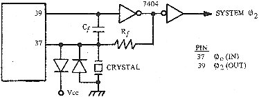 MCS6502 Parallel Mode Crystal Controlled Oscillator
FIGURE 1.16a
MCS6502 Parallel Mode Crystal Controlled Oscillator
FIGURE 1.16a
 MCS6502 Series Mode Crystal Controlled Oscillator
FIGURE 1.16b
MCS6502 Time Base Generation - Crystal Controlled
FIGURE 1.16
MCS6502 Series Mode Crystal Controlled Oscillator
FIGURE 1.16b
MCS6502 Time Base Generation - Crystal Controlled
FIGURE 1.16
 MCS6502 Time Base Generator - RC Network
FIGURE 1.17
-43-
MCS6502 Time Base Generator - RC Network
FIGURE 1.17
-43-
circuit. Values of the feedback resistor, RF, and feedback capacitor, CF, will be different for the crystal mode versus the RC mode. while the de- tail specifications for values of RF and CF are found in the data sheet for the MCS6502, clock timing can be generated by use of combinations of RF in the range of 0 to 500K ohms and CF in the range of 2 to 12 pf. The reader is referred to the MCS6502 data sheet for a detailed description of the application of RC networks and crystal oscillators for generation of the time base in these modes of operation. The MCS6500 bus discipline described in Section 1.3.1 is appli- cable wherever the oscillator is located. For data transfers to be properly carried out between the processor and the various support chips in the sys- tems, the timing of the clocks controlling the internal processor opera- tions must be very close to that of the phase two clock out of pin 39 of the processor with no more than two TTL delays for clock buffering. It is important in systems which drive the clock generators with a TTL square wave that this input waveform not be used to control the peripheral chips unless care is taken to assure proper timing of the phase two clock being used in these support chips. 1.4.2.3 SYNC Signal In the MCS6502, a SYNC signal is provided to identify those cycles in which the processor is doing an OP CODE fetch. The SYNC line goes high during phase one of an OP CODE fetch and stays high for the remainder of that cycle. If the RDY line is pulled low during the phase one clock pulse in which the SYNC line went high, the processor will stop in its current state. It remains in that state until the RDY line goes high. In this manner, the SYNC signal can be used to control RDY to cause single-instruc- tion execution. This application is discussed in detail in Chapter 2. Figure 1.18 contains a timing diagram for this signal. 1.4.2.4 S.O.--Set Overflow This pin sets the overflow flag on a negative transition from TTL one to TTL zero. This is designed to work with a future I/O part and should not be used in normal applications unless the user has programmed for the fact the arithmetic operations also affect the overflow flag.
-44-
MCS6502 SYNC Signal FIGURE 1.18 -45-
The operation of each function is exactly the same as on the MCS6502. | | | | | | Features | MCS6503 | MCS6504 | MCS6505 | | | | | | | | | | | | | | | | | Addressing | 4096 Bytes | 8192 Bytes | 4096 Bytes | | Capability | (AB00 - AB11) | (AB00 - AB12) | (AB00 - AB11) | | | | | | | | | | | | Interrupt | ___ ___ | ___ | ___ | | Request | IRQ, NMI | IRQ | IRQ | | Capability | | | | | | | | | | | | | | | | | | | | "Ready" Signal | -- | -- | RDY | | | | | | | | | | | | Timing | Single Phase | Single Phase | Single Phase | | Signals | TTL Level Ø0(IN), | TTL Level Ø0(IN), | TTL Level Ø0(IN), | | Required | or Crystal or RC | or Crystal or RC | or Crystal or RC | | | | | | | | | | | | Other Control | ___ | ___ | ___ | | Signals | RES, R/W | RES, R/W | RES, R/W | | | | | |
Functional Features of MCS6503, MCS6504, MCS6505 FIGURE 1.19 -46-
Figure 1.20 illustrates the pin designation for the three proces- sors, indicating the tradeoffs that exist between control signals and ad- dressing capability due to pinout constraints. Like the MCS6502, the 28- pin microprocessors also have the on-the-chip-oscillator and clock drivers. Figure 1.21 and 1.22 display the circuitry necessary to generate the time base in the crystal mode and RC network mode respectively. Specific de- tails on the value of feedback resistance, RF, and feedback capacitance, CF, can be found in the appropriate data sheet.
-47-
 MCS6503, MCS6504, MCS6505 Pinout Designations
FIGURE 1.20
-48-
MCS6503, MCS6504, MCS6505 Pinout Designations
FIGURE 1.20
-48-
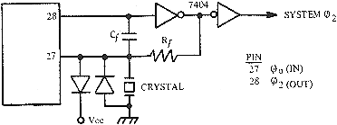 MCS6503,4,5 Parallel Mode Crystal
Controlled Oscillator
MCS6503,4,5 Parallel Mode Crystal
Controlled Oscillator
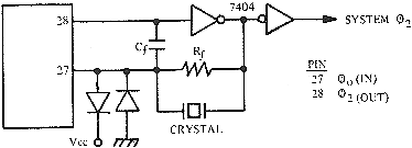 MCS6503,4,5 Series Mode Crystal
Controlled Oscillator
MCS6503, MCS6504, MCS6505 Time Base Generation
Crystal Controlled
FIGURE 1.21
MCS6503,4,5 Series Mode Crystal
Controlled Oscillator
MCS6503, MCS6504, MCS6505 Time Base Generation
Crystal Controlled
FIGURE 1.21
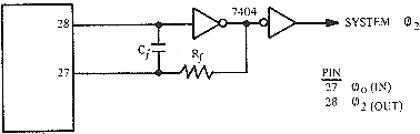 MCS6503, MCS6504, MCS6505 Time Base Generator
RC Network
FIGURE 1.22
-49-
MCS6503, MCS6504, MCS6505 Time Base Generator
RC Network
FIGURE 1.22
-49-
1.5 PERIPHERAL INTERFACE DEVICE - MCS6520 1.5.1 Introduction The MCS6520 is a direct pin for pin replacement for the Motorola MC6820 Peripheral Interface Adapter, the "PIA". As such, it meets all of the "PIA" electrical specifications and is totally hardware compatible with the MC6820. The MCS6520 is an I/O device which acts as an interface between the microprocessor and peripherals such as printers, displays, keyboards, etc. The prime function of the NG56520 is to respond to stimulus from each of the two worlds it is serving. On the one side, the MCS6520 is interfacing with peripherals via two eight-bit bi-directional peripheral data ports. On the other side, the device interfaces with the micropro- cessor through an eight-bit data bus; this is the same data bus discussed at length in Section 1.3.1. It is, therefore, simplest to view the basic function of the MCS6520 as in the block diagram of Figure 1.23.
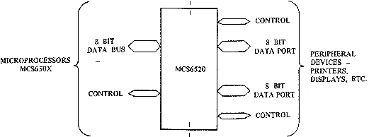 Basic MCS6520 Interface Diagram
FIGURE 1.23
-50-
Basic MCS6520 Interface Diagram
FIGURE 1.23
-50-
In addition to the lines described above, the MCS6520 provides four interrupt input/peripheral control lines and the logic necessary for simple, effective control of peripheral interrupts. No external logic is required for interfacing the MCS650X microprocessor to most peripheral devices. The functional configuration of the MCS6520 is programmed by the microprocessor during systems initialization. Each of the peripheral data lines is programmed to act as an input or output and each of the four control/interrupt lines may be programmed for one of four possible control modes. This allows a high degree of flexibility in the overall operation of the interface. Some of the more important features of the MCS6520 are the following. * Compatibility with the MCS650X microprocessors. * Eight-bit bi-directional data bus for communication with the microprocessor. * Two eight-bit bi-directional ports for interface to peripherals. * Two programmable control registers. * Two programmable Data Direction Registers. * Four individually controlled interrupt input lines - two usable as peripheral control outputs. * Handshake control logic for input and output peripheral operation. * High impedance three-state and direct transistor drive peripheral lines. * Program controlled interrupt and interrupt mask capability. 1.5.2 Organization of the MCS6520 Figure 1.25 contains a block diagram of the MCS6520 showing the internal registers and data paths and the various inputs and outputs on the device. This section contains a general description of the internal organization of the device along with a discussion of how the various registers affect one another. The following sections discuss the details
-51-
 MCS6520 Pinout Designations Peripheral Interface Adapter
FIGURE 1.24
-52-
MCS6520 Pinout Designations Peripheral Interface Adapter
FIGURE 1.24
-52-
 MCS6520 Internal Architecture
FIGURE 1.25
-53-
MCS6520 Internal Architecture
FIGURE 1.25
-53-
of the inputs and outputs on the chip, along with a detailed discussion of the operation of each register. The final section discusses the MCS6520 from an operational viewpoint, describing the interaction of the register bits, input/output lines, etc. The MCS6520 is organized into two independent sections referred to as the "A Side" and the "B Side." Each section consists of a Control Regis- ter (CRA, CRB), Data Direction Register (DDRA, DDRB), Output Register (ORA, ORB), Interrupt Status Control and the buffer necessary to drive the Periph- eral Interface busses. 1.5.2.1 Data Input Register When the microprocessor writes data into the MCS6520, the data which appears on the data bus during the Phase Two clock pulse is latched into the Data Input Register. It is then transferred into one of six in- ternal registers of the MCS6520 after the trailing edge of Phase Two. This assures that the data on the peripheral output lines will not "glitch," i.e., the output lines will make smooth transitions from high to low or from low to high and the voltage will remain stable except when it is going to the opposite polarity. 1.5.2.2 Control Registers (CRA and CRB) Figure 1.29 illustrates the bit designation and functions in the Control Registers. The Control Registers allow the microprocessor to con- trol the operation of the interrupt lines (CA1, CA2, CB1, CB2), and periph- eral control lines (CA2, CB2). A single bit in each register controls the addressing of the Data Direction Registers (DDRA, DDRB) and the Output Reg- isters (ORA, ORB) discussed below. In addition, two bits (bit 6 and 7) are provided in each control register to indicate the status of the interrupt input lines (CA1, CA2, CBl, CB2). These interrupt status bits (IRQA, IRQB) are normally interrogated by the microprocessor during the interrupt serv- ice program to determine the source of an active interrupt. These are the interrupt lines which drive the interrupt input (IRQ, NMI) of the micro- processor. The other bits in CRA and CRB are described in the discussion of the interface to the peripheral device (Section 1.5.4). The various bits in the control registers will be accessed many times during a program to allow the processor to enable or disable inter- rupts) change operating modes, etc. as required by the peripheral device being controlled.
-54-
1.5.2.3 Data Direction Registers (DDRA, DDRB) The Data Direction Registers allow the processor to program each line in the 8-bit Peripheral I/O port to act as either an input or an out- put. Each bit in DDRA controls the corresponding line in the Peripheral A port and each bit in DDRB controls the corresponding line in the Peripheral B port. Placing a "0" in the Data Direction Register causes the correspond- ing Peripheral I/O line to act as an input. A "1" causes it to act as an output. The Data Direction Registers are normally programmed only during the system initialization routine which is performed in response to a Reset signal. However, the contents of these registers can be altered during system operation. This allows very convenient control of some peripheral devices such as keyboards. 1.5.2.4 Peripheral Output Registers (ORA, ORB) The Peripheral Output Registers store the output data which ap- pears on the Peripheral I/O port. Writing an "0" into a bit in ORA causes the corresponding line on the Peripheral A port to go low (< 0.4v) if that line is programmed to act as an output. A "1" causes the corresponding output to go high. The lines of the Peripheral B port are controlled by ORB in the same manner. Addressing of these registers is discussed in Section 1.5.3.4. 1.5.2.5 Interrupt Status Control The four interrupt/peripheral control lines (CA1, CA2, CB1, CB2) are controlled by the Interrupt Status Control (A, B). This logic inter- prets the contents of the corresponding Control Register, detects active transitions on the interrupt inputs and performs those operations necessary to assure proper operation of these four peripheral interface lines. The operation of these lines is described in detail in Section 1.5.4.2. 1.5.2.6 Peripheral Interface Buffers (A, B) and Data Bus Buffers (DBB) The Buffers which drive the peripheral I/O ports and the data bus provide the current and voltage drive necessary to assure proper system operation and to meet the device specifications.
-55-
1.5.3 Interface Between MCS6520 and the MCS650X Family of Microprocessors The MCS6520 interfaces to the microprocessor with an 8-bit bi-direc- tional data bus, 3 chip-select lines, 2 register-select lines, 2 interrupt request lines, read/write line, enable line and reset line. 1.5.3.1 Data Bus (D0-D7) The 8-bit, bi-directional data bus allows the transfer of data be- tween the microprocessor and the MCS6520. The data bus output drivers are 3-state devices that remain in the high impedance state except when the microprocessor reads data from the peripheral adapter. This data bus is the same as discussed in Section 1.3.1, "Bus Structure." 1.5.3.2 Enable (E) The Enable input is the only microprocessor interface timing input on the peripheral interface device. All data transfers into and out of the MCS6520 are controlled by this signal. In normal operation, this input should be connected to the phase two clock signal. In the case of the MCS6501, this is the 02 clock generated external to the microprocessor chip. For on-chip oscillator products (MCS6502, MCS6503, MCS6504 and MCS6505), the enable pulse becomes 02(OUT). 1.5.3.3 Read/Write (R/W) This signal is generated by the microprocessor to control the di- rection of data transfers on the data bus. A low (< 0.4v) on this line enables the input buffers (microprocessor Write) and data is transferred from the microprocessor to the MCS6520 under control of Enable input if the device has been chip-selected. A high on the R/W line allows the MCS6520 to transfer data to the data bus buffers. The data bus buffers are enabled when the proper chip-select and Enable signals are present. Figure 1.26 illustrates the Read/Write timing. 1.5.3.4 Chip Select Lines (CS1, CS2, CS3) These three inputs allow the microprocessor to select the proper peripheral interface device. CS1 and CS2 must be high and CS3 must be low for selection of the device. Data transfers are then performed under con- trol of the Enable and R/W signals. These lines are normally connected to the address lines on the microprocessor, either directly or through address decoders.
-56-
 Microprocessor Interface Timing Read
FIGURE 1.26a
Microprocessor Interface Timing Read
FIGURE 1.26a
 *NOTE: ALL TIMES SPECIFIED ARE IN nSEC FOR 1MHZ OPERATION.
Microprocessor Interface Timing - Write
FIGURE 1.26b
-57-
*NOTE: ALL TIMES SPECIFIED ARE IN nSEC FOR 1MHZ OPERATION.
Microprocessor Interface Timing - Write
FIGURE 1.26b
-57-
As described in Section 1.5.5.2, a single bit in each Control Reg- ister (CRA and CRB) controls access to the Data Direction Register or the Peripheral interface. If bit 2 in the Control Register is a "1," a Periph- eral Output register (ORA, ORB) is selected, and if bit 2 is a "0," the Data Direction Register is selected. Internal registers are selected by the Register Select lines (RS0, RS1) and the Data Direction Register Access Control bit as follows: Data Direction Register Access Control Bit RS1 RS0 CRA-2 CRB-2 Register Selected 0 0 1 - Peripheral Interface A (See Section 1.5.3.5.1) 0 0 0 - Data Direction Register A 0 1 - - Control Register A 1 0 - 1 Peripheral Interface B (See Section 1.5.3.5.2) 1 0 - 0 Data Direction Register B 1 1 - - Control Register B If the programmer wishes to write the data into DDRA, ORA, DDRB, or ORB, he must first set bit 2 in the proper Control Register. The de- sired register can then be accessed with the address determined by the address interconnect technique used. (See Chapter 2, Section 2.3.1 for a discussion of addressing in MCS650X systems.) 1.5.3.5 Register Select Lines (RS0), (RS1) These two register select lines are used to select the various reg- isters inside the MCS6520. These input lines are used in conjunction with internal control registers to select a particular register that is to be accessed by the microprocessor. These lines are normally connected to microprocessor address output lines. These lines operate in conjunction with the chip-select inputs to allow the microprocessor to address a single 8-bit register. within the microprocessor address space. This register may be an internal register (CRA, ORA, etc.) or it may be a Peripheral I/O port. The processor can write directly into the Control Registers (CRA, CRB), the Data Direction Registers (DDRA, DDRB) and the Peripheral Output Registers (ORA, ORB). In addition, the processor can directly read the
-58-
contents of the Control Registers and the Data Direction Registers. Access- ing the Peripheral Output Register for the purpose of reading data back into the processor operates differently on the ORA and the ORB registers and therefore are discussed separately below. 1.5.3.5.1 Reading the Peripheral A I/O Port The Peripheral A I/O port consists of 8 lines which can be pro- grammed to act as inputs or outputs. When programmed to act as outputs, each line reflects the contents of the corresponding bit in the Peripheral Output Register. When programmed to act as an input, these lines will go high or low depending on the input data. The Peripheral Output Register (ORA) has no effect on those lines programmed to act as inputs. The 8 lines of the Peripheral A I/O port therefore contain either input or output data depending on whether the line is programmed to act as an input or an output. Figure 1.27a illustrates the interface timing. Performing a Read operation with RS1 = 0, RS0 = 0 and the Data Direction Register Access Control bit (CRA-2) = 1, directly transfers the data on the Peripheral A I/O lines into the processor (via the data bus). This will contain both the input and output data. The processor must be programmed to recognize and interpret only those bits which are important to the particular peripheral operation being performed. Since the processor always reads the Peripheral A I/O port pins instead of the actual Peripheral Output Register (ORA), it is possible for the data read into the processor to differ from the contents of the Periph- eral Output Register for an output line. This is true when the I/O pin is not allowed to go to a full +2.4v DC when the Peripheral Output register contains a logic 1. In this case, the processor will read a 0 from the Peripheral A pin, even though the corresponding bit in the Peripheral Out- put register is a 1. 1.5.3.5.2 Reading the Peripheral B I/O Port Reading the Peripheral B I/O port yields a combination of input and output data in a manner similar to the Peripheral A port. However, data is read directly from the Peripheral B Output Register (ORB) for those lines programmed to act as outputs. It is therefore possible to load down the Peripheral B Output lines without causing incorrect data to be trans- ferred back into the processor on a Read operation. Figure l.27b illus- trates the timing.
-59-
 Peripheral A Interface Timing
FIGURE 1.27a
-60-
Peripheral A Interface Timing
FIGURE 1.27a
-60-
 Peripheral A Interface Timing
FIGURE 1.27b
-61-
Peripheral A Interface Timing
FIGURE 1.27b
-61-
-63- -64- Peripheral I/O Fort A Buffer
FIGURE 1.28A
Peripheral I/O Fort A Buffer
FIGURE 1.28A
 Peripheral I/O Port B Buffer
FIGURE 1.28B
-62-
Peripheral I/O Port B Buffer
FIGURE 1.28B
-62-
The details of the Peripheral A and Peripheral B ports will be
discussed in the next section under the discussion of the interface between
the MCS6520 and the Peripheral Devices.
1.5.3.6 Reset (RES)
The active low Reset line resets the contents of all MCS6520 reg-
isters to a logic zero. This line can be used as a power-on reset or as a
master reset during system operation.
1.5.3.7 Interrupt Request Line (IRQA, IRQB)
The active low Interrupt Request lines (IRQA and IRQB) act to
interrupt the microprocessor either directly or through external interrupt
priority circuitry. These lines are "open source" (no load device on the
chip) and are capable of sinking 1.6 milliamps from an external source.
This permits all interrupt request lines to be tied together in a "wired-OR"
configuration. The "A" and "B" in the titles of these lines correspond to
the "A" peripheral port and the "B" peripheral port. Hence each interrupt
request line services one peripheral data port.
Each Interrupt Request line has two interrupt flag bits which can
cause the Interrupt Request line to go low. These flags are bits 6 and 7
in the two Control Registers. These flags act as the link between the
peripheral interrupt signals and the microprocessor interrupt inputs. Each
flag has a corresponding interrupt disable bit which allows the processor
to enable or disable the interrupt from each of the four interrupt inputs
(CA1, CA2, CB1, CB2).
The four interrupt flags are set by active transitions of the sig-
nal on the interrupt input (CA1, CA2, CB1, CB2). Controlling this active
transition is discussed in the next section under the discussion of the
interface between the MCS6520 and the peripheral device.
1.5.3.7.1 Control of IRQA
Control Register A bit 7 is always set by an active transition
of the CA1 interrupt input signal. Interrupting from this flag can be dis-
abled by setting bit 0 in the Control Register A (CRA) to a logic 0. Like-
wise, Control Register A bit 6 can be set by an active transition of the
CA2 interrupt input signal. Interrupting from this flag can be disabled by
setting bit 3 in the Control Register to a logic 0.
Both bit 6 and bit 7 in CRA are reset by a "Read Peripheral Out-
put Register A" operation. This is defined as an operation in which the
proper chip-select and register-select signals are provided to allow the
processor to read the Peripheral A I/O port.
1.5.3.7.2 Control of IRQB
Control of IRQB is performed in exactly the same manner as that
described above for IRQA. Bit 7 in CRB is set by an active transition on
CB1; interrupting from this flag is controlled by CRB bit 0. Likewise, bit
6 in CRB is set by an active transition on CB2; interrupting from this flag
is controlled by CRB bit 3.
Also, both bit 6 and bit 7 are reset by a "Read Peripheral B
Output Register" operation.
SUMMARY:
IRQA goes low when CRA-7 = 1 and CRA-0 = 1 or when CRA-6 = 1 and
CRA-3 = 1.
IRQB goes low when CRB-7 = 1 and CRB-0 = 1 or when CRB-6 = 1 and
CRB-3 = 1.
The use of these interrupt flags and interrupt disable bits is
discussed in more detail in Section 1.5.4.
It should be stressed at this point that the flags act as the
link between the peripheral interrupt signals and the processor interrupt
inputs. The interrupt disable bits allow the processor to control the
interrupt function.
1.5.4 Interface Between MCS6520 and Peripheral Devices
The MCS6520 provides 2 8-bit bi-directional ports and 4 interrupt/
control lines for interfacing to peripheral devices. These ports and the
associated interrupt/control lines are referred to as the "A" side and the
and the "B" side. Each side has its own unique characteristics and will
therefore be discussed separately below.
1.5.4.1 Peripheral I/O Ports
The peripheral A and Peripheral B I/O ports allow the microproces-
sor to interface to the input lines on the peripheral device by loading
data into the Peripheral Output Register. They also allow the processor to
interface with the peripheral device output lines by reading the data on
the Peripheral Port input lines directly onto the data bus and into the
internal registers of the processor.
1.5.1.1.1 Peripheral A I/O Port (PA0-PA7)
As discussed in Section 1.5.2.3. each of the Peripheral I/O lines
can be programmed to act as an input or an output. This is accomplished by
setting a "1" in the corresponding bit in the Data Direction Register for
those lines which are to act as outputs. A "0" in a bit of the Data Direc-
tion Register causes the corresponding Peripheral I/O lines to act as an
input.
The buffers which drive the Peripheral A I/O lines contain
"passive" pull-ups as shown in Figure 1.28a. These pull-up devices are
resistive in nature and therefore allow the output voltage to go to Vdd for
a logic 1. The switches can sink a full 1.6 ma, making these buffers cap-
able of driving one standard TTL load.
In the input mode, the pull-up devices shown in Figure 1.28a are
still connected to the I/O pin and still supply current to this pin. For
this reason, these lines represent one standard TTL load in the input mode.
1.5.4.1.2 Peripheral B I/O Port (PB0-PB7)
The Peripheral B I/O port duplicates many of the functions of
the Peripheral A port. The process of programming these lines to act as an
input or an output has been discussed previously. Likewise, the effect of
reading or writing this port has been discussed. However, there are sev-
eral characteristics of the buffers driving these lines which affect their
use in peripheral interfacing. These will be discussed below.
The Peripheral B I/O port buffers are push-pull devices as shown
in Figure 1.28b. The pull-up devices are switched "OFF" in the "0" state
and "ON" for a logic 1. Since these pull-ups are active devices, the logic
"1" voltage is not guaranteed to go higher than +2.4V. They are TTL com-
patible but are not CMOS compatible.
However, the active pull-up devices can sink up to 1 ma at 1.5V.
This current drive capability is provided to allow direct connection to
Darlington transistor switches. This allows very simple control of relays,
lamps, etc.
Because these outputs are designed to drive transistors directly,
the output data is read directly from the Peripheral Output Register for
those lines programmed to act as inputs.
-65-
The final characteristic which is a function of the Peripheral B push-pull buffers is the high-impedance input state. When the Peripheral B I/O lines are programmed to act as inputs, the output buffer enters the high impedance state. These inputs will then have an impedance of greater than 1 megohm. 1.5.4.2 Interrupt Input/Peripheral Control Lines (CA1, CA2, CB1, CB2) The four interrupt input/peripheral control lines provide a number of special peripheral control functions. These lines greatly enhance the power of the two general purpose interface ports (PA0-PA7, PB0-PB7). 1.5.4.2.1 Peripheral A Interrupt Input/Peripheral Control Lines (CA1, CA2) CA1 is an interrupt input only. An active transition of the signal on this input will set bit 7 of the Control Register A to a logic 1. The active transition can be programmed by the microprocessor by setting a "0" in bit 1 of the CRA if the interrupt flag (bit 7 of CRA) is to be set on a negative transition of the CA1 signal or a "1" if it is to be set on a positive transition. Note: A negative transition is defined as a trans- ition from a high (> 2.4v) to a low (< 0.4V), and a positive transition is defined as a transition from a low to a high voltage. Setting the interrupt flag will interrupt the processor through IRQA if bit 0 of CRA is a 1 as described previously. CA2 can act as a totally independent interrupt input or as a peripheral control output. As an input (CRA, bit 5 = 0) it acts to set the interrupt flag, bit 6 of CRA, to a logic 1 on the active transition selec- ted by bit 4 of CRA. These control register bits and interrupt inputs serve the same basic function as that described above for CA1. The input signal sets the interrupt flag which serves as the link between the peripheral device and the processor interrupt structure. The interrupt disable bit allows the processor to exercise control over the system interrupts. In the Output mode (CRA, bit 5 = 1), CA2 can operate indepen- dently to generate a simple pulse each time the microprocessor reads the data on the Peripheral A I/O port. This mode is selected by setting CRA, bit 4 to a 0 and CRA, bit 3 to a "1." This pulse output can be used to control the counters, shift registers, etc. which make sequential data available on the Peripheral input lines.
-66-
A second output mode allows CA2 to be used in conjunction with CA1 to "handshake" between the processor and the peripheral device. On the A side, this technique allows positive control of data transfers from the peripheral device into the microprocessor. The CA1 input signals the pro- cessor that data is available by interrupting the processor. The processor reads the data and sets CA2 low. This signals the peripheral device that it can make new data available. This technique is discussed in detail in Chapter 2. The final output mode can be selected by setting bit 4 of CRA to a 1. In this mode, CA2 is a simple peripheral control output which can be set high or low by setting bit 3 of CRA to a 1 or a 0 respectively. The operation of CA1 and CA2 is summarized in the next section. 1.5.4.2.2 Peripheral B Interrupt Input/Peripheral Control Lines (CB1, CB2) CB1 operates as an interrupt input only in the same manner as CA1. Bit 7 of CRB is set by the active transition selected by bit 0 of CRB. Likewise, the CB2 input mode operates exactly the same as the CA2 input modes. The CB2 output modes, CRB, bit 5 = 1, differ somewhat from those of CA2. The pulse output occurs when the processor writes data into the Periph- eral B Output Register. Also, the "handshaking" operates on data transfers from the processor into the peripheral device. The operation of CB1 and CB2 is summarized in the next section. A more detailed discussion of handshaking on the Peripheral B I/O port is contained in Chapter 2 of this manual. 1.5.5 Summary of MCS6520 Operation 1.5.5.1 Control Register Operation
| | | | | CRA (CRB) | | | | | Active Transition | IRQA (IRQB) | | Bit 1 Bit 0 | of Input Signal* | Interrupt Outputs | | | | | | | | | | 0 0 | negative | Disable--remain high | | | | | | | | Enabled--goes low when bit 7 | | | | in CRA (CRB) is set by active | | 0 1 | negative | transition of signal on CA0 | | | | (CBI) | | | | | | 1 0 | positive | Disable--remain high | | | | | | 1 1 | positive | Enable--as explained above | | | | | | | | | | | | *Note 1: Bit 7 of CRA (CRB) will he set to a logic 1 by an active | | transition of the CA1 (CB1) signal. This is independent | | of the state of Bit 0 in CRA (CRB) | | | Control of interrupt Inputs CA1, CB1 FIGURE 1.30 | | | | | CRA (CRE) | | | | | Active Transition | IRQA (IRQB) | | Bit 5 Bit 4 Bit 3 | of Input Signal* | Interrupt Output | | | | | | | | | | | | | | 0 0 0 | negative | Disable--remains high | | | | | | | | Enabled--goes low when bit 6 | | | | in CRA (CRB) is set by active | | 0 0 1 | negative | transition of signal on CA2 | | | | (CB2) | | | | | | 0 1 0 | positive | Disable--remains high | | | | | | 0 1 1 | positive | Enable--as explained above | | | | | | | | *Note: Bit 6 of CRA (CRB) will be set to a logic 1 by an active | | transition of the CA2 (CB2) signal. This is independent | | of the state of Bit 3 in CRA (CRB). | | | Control of CA2 (CB2) as Interrupt Inputs (Bit 5 "0") FIGURE 1.31a -68-
| | | | | CRA | | | | Bit 5 Bit 4 Bit 3 | Mode | Description | | | | | | | | | | | | CA2 is set high on an active | | | | transition of the CA1 interrupt | | | | input signal and set low by a | | 1 0 0 | "Handshake" | microprocessor "Read A Data" | | | on Read | operation. This allows posi- | | | | tive control of data transfers | | | | from the peripheral device to | | | | the microprocessor. | | | | | | | | CA2 goes low for one cycle | | | | after a "Read A Data" opera- | | 1 0 1 | Pulse Output | tion. This pulse can be used | | | | to signal the peripheral de | | | | vice that data was taken. | | | | | | 1 1 0 | Manual Output | CA2 set low | | | | | | 1 1 1 | Manual Output | CA2 set high | | | | | Control of CA2 Output Modes FIGURE 1.31b | | | | | CRB | | | | Bit 5 Bit 4 Bit 3 | Mode | Description | | | | | | | | | | | | CB2 is set low on microproces | | | | sor "Write B Data" operation | | | | and is set high by an active | | 1 0 0 | "Handshake" | transition of the CB1 interrupt | | | on Write | input signal. This allows posi-| | | | tive control of data transfers | | | | from the microprocessor to the | | | | peripheral device. | | | | | | | | CB2 goes low for one cycle after| | | | a microprocessor "Write B Data" | | 1 0 1 | Pulse Output | operation. This can be used to | | | | signal the peripheral device | | | | that data is available. | | | | | | 1 1 0 | Manual Output | CB2 set low | | | | | | 1 1 1 | Manual Output | CB2 set high | | | | | Control of CB2 Output Modes FIGURE 1.31c -69-
1.5.5.2 MCS6520 Operation in MC6500 Systems A brief review of the overall operation of the MCS6520 should serve to tie together many of the details discussed previously. During the system initialization routine which is executed in response to the processor RESET signal, the microprocessor will write a pattern of 1's and 0's into the Data Direction Registers. This will determine those lines which are to act as inputs and those which are to act as outputs. This pattern will usually be fixed for the system operation. Therefore, the next step would be to set the various operating modes, active transitions, etc. which are controlled by the Control Registers. At the same time the Data Direction Register Access Control Bit can be set to a 1 to allow the processor to control the Peripheral Ports during system operation. The interrupts will normally remain disabled until the entire system is initialized. At this time, the interrupts are enabled and full system operation begins. During system operation, the microprocessor will interrogate the switches, sensors, etc. in the peripheral device by reading the data on the Peripheral Input lines. Binary or decimal data may he transferred into the microprocessor in the same way. At the same time the various lights, motors, solenoids, etc. on the peripheral device are controlled by writing data into the appropriate bits of the Peripheral Output Registers. The entire sequence of operations is determined by the programmer to control a particular periph- eral device in a defined manner. The various registers, gates, etc. in the Interface Device act primarily as a link between the internal processor oper- ations and the various inputs and outputs on the peripheral devices being controlled.
-70-
1.6 PERIPHERAL INTERFACE/MEMORY DEVICE - MCS6530 1.6.1 Introduction The MCS6530 is designed to operate in conjunction with the MCS650X Microprocessor. It is comprised of a mask programmable 1024 x 8 ROM, a 64 x 8 RAM, two 8 bit bi-directional ports capable of directly inter- facing the Microprocessor unit and peripheral devices and a programmable interval timer with interrupt, capable of timing in various intervals from 1 to 262,144 clock periods. The I/O configuration, the interval timer and interrupt capability are under software control. * 8 bit bi-directional Data Bus for communication with the microprocessor unit. * Two 8 bit bi-directional ports for direct interface to peripherals. * Two I/O Peripheral Data Direction Registers * Programmable Interval Timer from 1 to 256 x 1024 clock periods. * Programmable Interval Timer Interrupt * C MOS Compatible Peripheral Lines * Peripheral Pins with Direct Transistor Drive Capability * Three-State Data Pins * Up to 7K contiguous ROM with no external decoding * 1024 x 8 ROM * 64 x 8 Static RAM 1.6.2 Pinout Description Figure 1.33 is the pinout diagram of the MCS6530. 1.6.2.1 Reset (RES) During system initialization a Logic "O" on the RES input will cause a zeroing of all I/O registers. This in turn will cause all I/O buses to act as inputs thus protecting external components from possible damage and erroneous data while the system is being configured under software control. The Data Bus Buffers are put into an OFF-STATE during Reset. Interrupt is disabled when reset. The RES signal must be held low for at least one clock period when reset is required.
-71-
 MCS6530 Pinout Designation
FIGURE 1.32
-72-
MCS6530 Pinout Designation
FIGURE 1.32
-72-
1.6.2.2 Input Clock The input clock is a system Phase Two clock which can be either a low level clock (VIL < 0.4, VIH > 2.4) or high level clock (VIL < 0.2, +.3 VIH = Vcc-.2). 1.6.2.3 Read/Write (R/W) The R/W signal is supplied by the microprocessing unit and is used to control the transfer of data to and from the micraprocessing unit and the MCS6530. A high on the R/W pin allows the processor to read (with pro- per addressing) the data supplied by the MCS6530. A low on the R/W pin allows a write (with proper addressing) to the MCS6530. 1.6.2.4 Interrupt Request (IRQ) The IRQ pin is an interrupt pin from the interval timer. This same pin, if not used as an interrupt, can be used as a peripheral I/O pin (PB7). When used as an interrupt, the pin should be set up as an input by the data direction register. The pin will be normally high with a low indi- cating an interrupt from the MCS6530. An external pull-up device is not required; however, if collector-OR'd with other devices, the internal pull- up may be omitted with a mask option. 1.6.2.5 Data Bus (D0-D7) The MCS6530 has eight bi-directional data pins (D0-D7). These pins connect to the system's data lines and allow transfer of data to and from the microprocessor unit. The output buffers remain in the off state except when a Read operation occurs. 1.6.2.6 Peripheral Data Ports The MCS6530 has 16 pins available for peripheral I/O operations. Each pin is individually software programmable to act as either an input or an output. The 16 pins are divided into 2 8-bit ports, PA0-PA7 and PB0-PB7 PB5, PB6 and PB7 also have other uses which will be discussed in Section 1.6.4. The pins are set up as an input by writing a "0" into the corre- sponding bit in the data direction register. A "1" into the data direction register will cause its corresponding bit to be an output. When in the input mode, the peripheral output buffers are in the "1" state and a pull-up device acts as less than one TTL load to the peripheral data lines. On a Read operation, the microprocessor unit reads the peripheral pin. When the
-73-
peripheral device gets information from the MCS6530 it receives data stored in the data register. The microprocessor will read correct information if the peripheral lines are greater than 2.0 volts for a "1" and less than 0.8 volts for a "0" as the peripheral pins are all TTL compatible. Pins PA0 and PB0 are also capable of sourcing 3 mA at 1.5V, thus making them capable of Darlington drive. 1.6.2.7 Address Lines (A0-A9) There are 10 address pins. In addition to these 10, there is the ROM SELECT pin. The above pins, A0-A9 and ROM SELECT, are always used as addressing pins. There are 2 additional pins which are mask programmable and can be used either individually or together as CHIP SELECTS. They are pins PB5 and PB6. When used as peripheral data pins they cannot be used as chip selects. 1.6.3 Internal Organization A block diagram of the internal architecture is shown in Figure 1.33. The MCS6530 is divided into four basic sections, RAM, ROM, I/O and TIMER. The RAM and ROM interface directly with the microprocessor through the sys- tem data bus and address lines. The I/O section consists of 2 8-bit halves. Each half contains a Data Direction Register (DDR) and an I/O Register. The DDR controls the peripheral output buffers. A "1" written into the DDR sets up the corresponding peripheral buffer as an output buffer. By this, it is meant that anything then written into the I/O Register will appear on that corresponding peripheral pin. A "0" written into the DDR inhibits the output buffer from transmitting data from the I/O Register. The output buffer remains in the high state making it ready to receive data on the peripheral lines. It should be noted that the microprocessor, when reading the I/O Register, is in fact reading the Peripheral Pin and not the I/O Register. The only way the I/O Register data can be changed is by a microprocessor Write operation. The Register is not affected by the data on the Periph- eral Pin. 1.6.3.1 ROM--1K Byte (8K Bits) The 8K ROM is in a 1024 x 8 configuration. Address lines A0-A9, as well as RS0 are needed to address the entire ROM. With the addition of
-74-
 MCS6530 Internal Architecture
FIGURE 1.33
-75-
MCS6530 Internal Architecture
FIGURE 1.33
-75-
CS1 and CS2, up to seven MCS6530s may be addressed, giving 7168 x 8 bits of contiguous ROM. 1.6.3.2 RAM--64 Bytes (512 Bits) A 64 x 8 static RAM is contained on the MCS6530. It is addressed by A0-A5 (Byte Select), RS0, A6, A7, A8, A9 and, depending on the number of chips in the system, CS1 and CS2. 1.6.3.3 Internal Peripheral Registers There are four internal registers, two data direction registers and two peripheral I/O data registers. The two data direction registers (A side and B side) control the direction of data into and out of the periph- eral pins. For example, a "1" loaded into data direction register A, posi- tion 3 sets up peripheral pin PA3 as an output. If a "0" had been loaded instead, PA3 would be configured as an input. The two data I/O registers are used to latch data from the data bus during a Write operation until the peripheral device can read the data supplied by the microprocessor unit. Although during a Read operation the microprocessor unit reads the periph- eral pin, the address is the same as the register. For those pins pro- grammed as outputs by the data direction registers, the data on the pins will be the same as that in the I/O register. 1.6.3.4 Interval Timer The Timer section of the MCS6530 contains three basic parts: pre- liminary divide down register, programmable 8-bit register and interrupt logic. These are illustrated in Figure 1.34. The interval timer can be programmed to count up to 256 time intervals. Each time interval can be either 1T, 8T, 64T or 1024T incre- ments, where T is the system clock period. When a full count is reached, an interrupt flag is set to a logic "1." After the interrupt flag is set the internal clock begins counting down to a maximum of -255T. Thus, after the interrupt flag is set, a Read of the timer will tell how long since the flag was set up to a maximum of 255T. When writing to the timer, the high order 8 bits of the timer are written by the system data bus. If a count of 52 time intervals were to be counted, 0 0 1 1 0 1 0 0 would be written into the timer section. The time intervals of 1, 8, 64 or 1024T are decoded from address lines A0 and A1 at this same time. Address line A3, if high during this write operation,
-76-
 Basic Elements of Interval Timer
FIGURE 1.34
-77-
Basic Elements of Interval Timer
FIGURE 1.34
-77-
enables the interrupt flag onto pin PB7. PB7 should be programmed as an input if it is to be used as an interrupt pin. PB7 goes low when an inter- rupt occurs. When the timer is read prior to the interrupt flag being set, the number of time intervals remaining will be read, i.e., 51, 50, 49, etc. Should the timer be read when interrupt occurs, the value read would be 1 1 1 1 1 1 1 1. After interrupt, the timer register decrements at a divide by "1" rate of the system clock. If after interrupt, the timer is read and a value of 1 1 1 0 0 1 0 0 is read, the time since interrupt is 28T. The value read is in two's complement. Value read = 1 1 1 0 0 1 0 0 Complement = 0 0 0 1 1 0 1 1 ADD 1 = 0 0 0 1 1 1 0 0 = 28. Thus, to arrive at the total elapsed time, merely do a two's complement add to the original time written into the timer. Again, assume time written as 0 0 1 1 0 1 0 0 (= 52). With a divide by 8, total time to interrupt is (52 x 8) + 1 = 417T. Total elapsed time would be 416T + 28T = 444T, assum- ing the value read after interrupt was 1 1 1 0 0 1 0 0. After interrupt, whenever the timer is written or read the inter- rupt is reset. However, the reading or writing of the timer at the same time interrupt occurs will not reset the interrupt flag. Figure 1.35 illustrates an example of interrupt. When reading the timer after an interrupt, A3 should be low so as to disable the IRQ pin. This is done so as to avoid future interrupts until after another Write timer operation. 1.6.4 Addressing Addressing of the MCS6530 offers many variations to the user for greater flexibility. The user may configure his system with RAM in lower memory, ROM in higher memory, and I/O registers with interval timers between the extremes. There are 10 address lines (A0-A9). In addition, there is the possibility of 3 additional address lines to be used as chip-selects and to distinguish between ROM, RAM, I/O and interval timer. Two of the addi- tional lines are chip-selects 1 and 2 (CS1 and CS2). The chip-select pins can also be PB5 and PB6. Whether the pins are used as chip-selects or peripheral I/O pins is a mask option and must be specified when ordering the part. Both pins act independently of each other in that either or both
-78-
pins may be designated as a chip-select. The third additional address line is RS0. The MCS6502 and MCS6530 in a 2-chip system would use RS0 to dis- tinguish between ROM and non-ROM sections of the MCS6530. With the ad- dressing pins available, a total of 7K contiguous ROM may be addressed with no external decode. Below is an example of a 1-chip and a 7-chip MCS6530 Addressing Scheme. 1.6.4.1 One-Chip Addressing Figure 1.36 illustrates a 1-chip system decode for the MCS6530. 1.6.4.2 Seven-Chip Addressing In the 7-chip system the objective would be to have 7K of contigu- ous ROM, with RAM in low order memory. The 7K of ROM could be placed be- tween addresses 65,536 and 1024. For this case, assume A13, A14 and A15 are all 1 when addressing ROM, and 0 when addressing RAM or I/O. This would place the 7K ROM between Addresses 65,535 and 57,367. The 2 pins designated as chip-select or I/O would be masked programmed as chip-select pins. Pin RS0 would be connected to address line A10. Pins CS1 and CS2 would be connected to address lines A11 and A12 respectively. See Figure 1.37. The two examples shown would allow addressing of the ROM and RAM; however, once the I/O timer has been addressed, further decoding is necs- sary to select which of the I/O registers are desired, as well as the cod- ing of the interval timer. 1.6.4.3 I/O Register--Timer Addressing Figure 1.38 illustrates the addressing decoding for the internal elements and timer programming. Address line A2 distinguishes I/O regis- ters from the timer. When A2 is low and I/O timer select is high, the I/O registers are addressed. Once the I/O registers are addressed, address lines A1 and A0 decode the desired register. When the timer is selected A1 and A0 decode the divide by matrix. This is discussed further in the Timer Section. In addition, Address A3 is used to enable the interrupt flag to PB7.
-80-
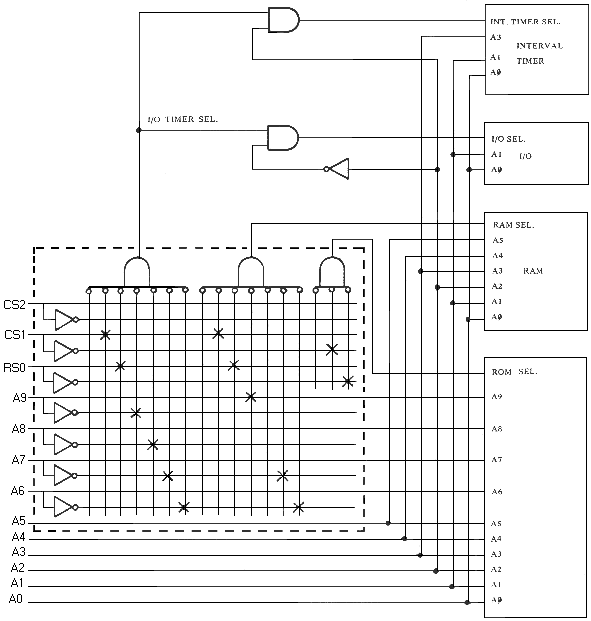
The addressing of the ROM select, RAM select and I/O Timer select lines would be as follows: CS2 CS1 RS0 A12 A11 A1O A9 A8 A7 A6 MCS6530 #1, ROM SELECT 0 0 1 X X X X RAM SELECT 0 0 0 0 0 0 0 I/O TIMER 0 0 0 1 0 0 0 MCS6530 #2, ROM SELECT 0 1 0 X X X X RAM SELECT 0 0 0 0 0 0 1 I/O TIMER 0 0 0 1 0 0 1 MCS6530 #3, ROM SELECT 0 1 1 x x x x RAM SELECT 0 0 0 0 0 1 0 I/O TIMER 0 0 0 1 0 1 0 MCS6530 #4, ROM SELECT 1 0 0 X X X X RAM SELECT 0 0 0 0 0 1 1 I/O TIMER 0 0 0 1 0 1 1 MCS6530 #5, ROM SELECT 1 0 1 X X X X RAM SELECT 0 0 0 0 1 0 0 I/O TIMER 0 0 0 1 1 0 0 MC56530 #6, ROM SELECT 1 1 0 x x x x RAM SELECT 0 0 0 0 1 0 1 I/O TIMER 0 0 0 1 1 0 1 MCS6530 #7, ROM SELECT 1 1 1 x x x x RAM SELECT 0 0 0 0 1 1 0 I/O TIMER 0 0 0 1 1 1 0
* RAM select for MCS6530 #5 would read = A12.A11.A10.A9.A8.A7.A6 MCS6530 Seven Chip Addressing Scheme FIGURE 1.37 -82-
ADDRESSING DECODE ROM SELECT RAM SELECT I/O TIMER SELECT R/W A3 A2 A1 A0 READ ROM 1 0 0 1 x x x x WRITE RAM 0 1 0 0 x x x x READ RAM 0 1 0 1 X X X X WRITE DDRA 0 0 1 0 X 0 0 1 READ DDRA 0 0 1 1 X 0 0 1 WRITE DDRB 0 0 1 0 X 0 1 1 READ DDRB 0 0 1 1 X 0 1 1 WRITE PER. REG. A 0 0 1 0 x 0 0 0 READ PER. REG. A 0 0 1 1 X 0 0 0 WRITE PER. REG. B 0 0 1 0 x 0 1 0 READ PER. REG. B 0 0 1 1 x 0 1 0 WRITE TIMER : 1T W/IRQ to PB7 0 0 1 0 1 1 0 0 : 8T WO/IRQ to PB7 0 0 1 0 0 1 0 1 : 64T WIIRQ to PB7 0 0 1 0 1 1 1 0 : 1024T WO/IRQ to PB7 0 0 1 0 0 1 1 1 READ TIMER DISABLE IRQ TO PB7 0 0 1 1 0 1 x 0 READ INTERRUPT FLAG 0 0 1 1 X 1 x 1
Addressing Decode for I/O Register and Timer FIGURE 1.38 -83-
CHAPTER 2 CONFIGURING THE MICROCOMPUTER SYSTEM
2.1 THE SYSTEM CONFIGURATION TASK The first part of any microprocessor-based design effort is the system con- figuration task. In fact, this probably requires more creativity from the de- signer than any other part of the design effort. The goal of the system con- figuration effort is the generation of a list of components which will make up the system, a detailed interconnect diagram and a detailed description of the total system operation. This includes a definition of how the processor will control the peripheral devices as well as a definition of the internal opera- tions to be performed. This does not include detailed implementation of the design such as laying out printed circuit boards and writing programs, but does involve enough analysis of the total operation to assure that the system will operate properly after all the hardware and software is assembled. The technically based selection of components and the definition of the general operation of the system must be based on consideration of two factors. These are: 1. System speed requirements 2. System input/output requirements Both of these factors are interrelated. Therefore, it will usually be necessary to define an I/O configuration and then verify that the processor can operate at the speed required by the peripheral devices. If there appears to be any diffi- culty with the I/O operation, this structure must be re-defined and re-analyzed. In addition to the speed requirements of the I/O devices, there are also general speed requirements for the internal processor operations (arithmetic operations, data manipulation, etc.). This speed requirement is usually some- what more flexible than that associated with I/O but it should be defined along with any other system requirements. The ultimate test of system speed must wait for the generation of both the hardware and the program; however, the system requirements and capability must be analyzed very early in the system develop- ment process to assure that no problems will arise during the last stages of the design.-84-
2.2 INPUT/OUTPUT TECHNIQUES 2.2.1 The General Purpose Input/Output (I/O) Port Although the concept of the I/O port was introduced briefly in Sec- tion 1, and the operation of two MCS6500 family devices which provide gen- eral purpose I/O capability has been discussed in Sections 1.5 and 1.6, little has been said about what factors must be considered when configur- ing an I/O structure using these devices. The general purpose I/O port consists of eight lines, each of which can act as either an input or an output. As an input, each line can detect the state of one switch or can detect one bit of data. As an output, each line can control one light, solenoid, etc. or can provide one bit of data to a peripheral device. If this technique is used in peripheral control, the operation of each line is totally defined in the system program. For most systems, the general purpose interface device provides more than adequate speed and flexibility to solve the entire peripheral inter- face problem. Usually, a cost savings can be realized because of the re- duced component cost and the necessity of stocking only one type of inter- face device. In addition, use of the general purpose peripheral interface device allows the designer to tailor the operation of the interface device to fit the problem at hand. The ultimate component selection must be preceded by a study of each section of the system input/output structure and a study of the overall sys- tern performance. Ultimately, the set of general purpose and special purpose peripheral interface devices selected for a system must be chosen to mini- mize total cost while assuring satisfactory system performance.
-85-
Processor speed is a function of two things. The first is simply the num- ber of instructions required to perform the desired operations. The second is the percentage of processor time required to service interrupts. The typical system may employ several interrupt signals which occur at fixed intervals. At times, these may be combined with other interrupts being generated by a periph- eral device. It is important that the total service time for these interrupts does not exceed that allowable and that the time available to the processor for executing the main program is sufficient to allow the system to operate at its required speed. During the system configuration process, detailed system programs need not be generated. However, it will be necessary to write small portions of the software to verify the speed of execution and to assure proper operation of the total system. This chapter will discuss special techniques for the control of the various components which may be included in a microcomputer system, as well as techniques for controlling peripheral devices which are attached to the system. A discus- sion of programming techniques which can be used to optimize the total system performance is contained in the Programming Manual. 2.2.2 The Special Purpose Peripheral Interface Device The special purpose, dedicated I/O device must also be considered in any microcomputer design. These devices are designed to completely handle a single well-defined problem; for example, driving a particular printer, handling a particular type of communications line or driving a scanned dis- play. These special purpose devices are designed to totally handle their particular task with very little help from the processor.
-86-
The primary advantage of this type of interface device is that it requires an absolute minimum amount of attention from the processor. The major disadvantage of special purpose I/O is increased component cost. The total production volume for these devices is less than that of the more universal I/O chips and also the total chip size is usually greater. The use of special purpose peripheral control devices will not be discussed in this manual. Instead, a detailed study will be made of the more general problem of configuring the 8-bit bi-directional peripheral port. In addition, this chapter will cover some special techniques which can greatly enhance the power of this type of interface device. 2.2.3 Configuring the General Purpose I/O Port The 8-bit peripheral control port included on the MCS6520 and the MCS6530 allows each line to be programmed to act as an input or an output. This is accomplished when the processor writes a pattern of 1's and 0's into the data direction register. Writing a 1 causes the pin to become an output, and writing a 0 causes it to act as an input. Although this opera- tion is normally performed only during system initialization, the ability to do so under program control allows some very important peripheral con- trol techniques. An example of this is described below. The process of configuring the general purpose I/O port involves first examining the peripheral devices to analyze the various control in- puts, switches, sensors, data signals, etc. which must be handled by the microprocessor to properly control the device. Each function must then be assigned to a line on the I/o port. The ultimate goal of this process is the creation of a list of I/O pins, the function of each pin, and an indi- cation of whether each pin is to be an input or an output. Since each line is capable of operating as an input or an output, and since there is very little to differentiate one line from any other, the actual assignment can be made fairly late in the system development cycle after consideration of software techniques and printed circuit board layout. In fact, software considerations may be the only thing which dic- tates that a signal be connected to one pin or another. Developing a thorough understanding of the software in the MCS6500 systems will require a detail study of the Programming Manual. However, several operations which can be performed by the processor and which affect the assignment of inputs and outputs will be discussed briefly here.
-87-
2.2.3.1 Assignment of Outputs A major factor in the assignment of output pins can be the ability of the MCS650X processor to increment and decrement memory. Since the I/O port is treated as a location in memory, this incrementing and decrementing can be used to rapidly set and clear the low order bit in this memory loca- tion. This is illustrated in Figure 2.1. Note that this does not affect anything but the low order bit if it is used properly as shown. This operation can be performed more rapidly than several other software techniques which can be used to affect a single bit. Therefore, control of a single indicator, data line, etc. can be greatly enhanced by putting it on the low order bit of an I/O port. This is the reason the low order bit of both the NC56530 peripheral ports (PA0 and PBO) provide the ability to drive transistors directly. In many appli- cations, a simple transistor attached to one of those pins would provide very convenient control of a motor, lamp, etc. The ability of the microprocessor to shift data in memory can be another very important factor in the assignment of outputs. Operations which require sequential strobe signals can be controlled conveniently by shifting a single high (or low) signal from pin to pin under software con- trol. The specific choice of pins can greatly enhance the ease with which this signal is controlled. 2.2.3.2 Assignment of Inputs In general, the processor deals with the input data from switches, keyboards, etc. by reading the data on the I/O port into the internal regis- ters of the processor (usually the accumulator) and using the resulting con- dition of flags in the Processor Status Register to control the program which is executed. During this transfer process, the N flag in the Proces- sor Status Register is set equal to the high order bit (bit 7) of the word read from the I/O port. This N flag can then be used to cause the processor to execute different sections of the program (See the Programming Manual, Chapter 4, for a detailed discussion of Branching). Likewise, by perform- ing certain instructions, the V flag in the Processor Status Register can be Set equal to bit 6 on the I/O port. This flag can then be used to affect the program which is executed. This operation of setting the internal flags from bits 6 and 7 of the memory word means that making these two lines inputs on an I/O port
-88-
MCS6S20 DATA REGISTER 1 LOADED INTO | | | | | | | | | VOLTAGE ON OUTPUT MCS6520 --->| 0 | 1 | 0 | 0 | 1 | 0 | 0 | 1 | PINS OF MCS6520 MICROPROCESSOR | | | | | | | | | | | +--------> HIGH (>2.4V) | +------------> LOW (<0.4V) +----------------> LOW 2 AFTER | | | | | | | | | DECREMENT --->| 0 | 1 | 0 | 0 | 1 | 0 | 0 | 0 | OPERATION | | | | | | | | | | | +--------> LOW | +------------> LOW +----------------> LOW 3 AFTER | | | | | | | | | SUBSEQUENT --->| 0 | 1 | 0 | 0 | 1 | 0 | 0 | 1 | INCREMENT | | | | | | | | | OPERATION | | +--------> HIGH | +------------> LOW +----------------> LOW
will allow very convenient testing of the condition of the switches, sensors, etc. attached to these inputs. If more than two input signals are to be attached to a port, the additional inputs should be placed on bit 5, then bit 4 and so on. The processor can then perform operations which shift the lower order bits into bit 7 one at a time and sets the N flag equal to this bit. After each shift the N flag can be used to determine the actual program which is to be executed. (See the Programming Manual for a discussion of the Shift instructions.) From the above example, one should conclude that the assignments which the designer makes will be very much a function of the software tech- niques which will be employed in controlling each line. It is very import- ant that the designer be familiar with these techniques and that he docu- ment the techniques which he has in mind when making the assignments. This is particularly important when the system program is to be written by some- one else. Also, it is important that those doing the system development work constantly review the I/O structure to optimize the software in- volved as the system program is written. 2.2.4 Power-On Considerations Chapter 1, Section 1.3.3 discusses the operation of the system RESET function. Reference is made to the fact that this can be used to assure that all I/O lines come up in a known state when power is applied to the chip. Although this is a very important function, the designer must assure himself that this RESET state does not adversely affect the peripheral devices. This section describes some of the problems which can be encoun- tered when the system is reset and discusses several techniques which can be used to assure smooth power-up operation. The I/O lines of the MCS6530 and MCS6520 all enter the input state when the reset line goes to GND (< 0.4V). For the MCS6530 I/O lines, and for the Peripheral A port on the MCS6520, these pins will go to +5V DC (Vdd). This is due to the output structure on these pins. When these lines are in the input state, the output switch becomes an open circuit but the pull-up device continues to supply current to the pin. Figure 2.2 shows a peripheral port which is configured to drive two solenoids. These solenoids can be controlled properly after the system is initialized; however, when the manual reset switch is activated, both I/O
-90-
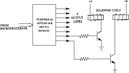 MCS6520 Control of Transistor Driven Solenoids
FIGURE 2.2
-91-
MCS6520 Control of Transistor Driven Solenoids
FIGURE 2.2
-91-
lines enter the input state, the transistors saturate (close) and the sole- noids are activated. This can be catastrophic in most mechanical subsys- tems, so it is important that this potential condition be understood and prevented. Figure 2.3 shows two satisfactory solutions to this problem. The first, Figure 2.3a, requires that a "0" be written into the output line by the processor to actuate the solenoids. This assures that the solenoids will not be powered simultaneously when the manual reset switch is pressed. However, it does introduce another potential problem. when the reset line on the peripheral interface device goes low (< 0.4V), the contents of both the Peripheral Data register and the Data Direction register are cleared to zeros. If the Data Direction register is set to 1's, both solenoids will immediately actuate due to the 0 stored in the Peripheral Data register. This can be avoided completely if the system software first sets the bits in the Peripheral Data register to a 1 and then sets the Data Direction register to a 1. The I/O pin will go high when the reset switch is actuated and will simply stay high through the initialization routine. Figure 2.3b illustrates a solution which may be more applicable to a large system or a complex peripheral. In this approach, a separate output line is used to apply power to the peripheral device. The power to the entire peripheral or to just the critical elements is kept off until the entire system is initialized and is ready to run the system program. On the MCS6520 Peripheral B port, the I/O lines are open circuit (high impedance) in the input state. As a result, the configuration in Figure 2.2 will not cause the same problem on the MCS6520 Peripheral B port as would be expected on the MCS6530. In the input state, the I/O pin is incapable of sourcing any more than a few microamps. However, if one were to use a solenoid driver as shown in Figure 2.4, the TTL input structure on the drivers would interpret the high-impedance state as a logic 1 and would actuate the solenoids. Both the solutions in Figure 2.3 would be satisfactory in this case. However, the transistors are connected to the TTL buffer. In addition, the extra output shown in Figure 2.3b, controlling power to the peripheral device, could actually be used to enable the solenoid drivers if an enable input is available to these devices. This configuration is illustrated in Figure 2.5.
-92-
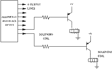 MCS6520 Control of PNP Transistor driving Solenoid Coil
FIGURE 2.3A
MCS6520 Control of PNP Transistor driving Solenoid Coil
FIGURE 2.3A
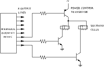 MCS6520 Controlling Both Power and Drivers of Solenoid Cell
FIGURE 2.3B
MCS6520 Controlling Both Power and Drivers of Solenoid Cell
FIGURE 2.3B
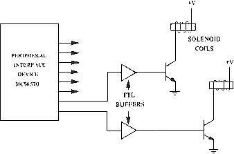 MCS6520 Driving TTL Buffers
FIGURE 2.4
-93-
MCS6520 Driving TTL Buffers
FIGURE 2.4
-93-
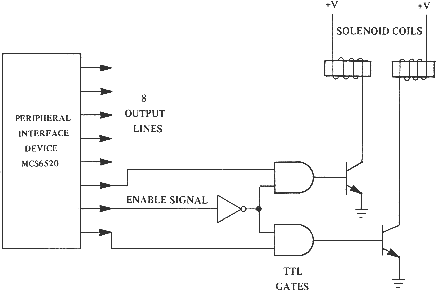 MCS6520 Controlling Solenoids with Enable Signal and TTL Interface
FIGURE 2.5
MCS6520 Controlling Solenoids with Enable Signal and TTL Interface
FIGURE 2.5
-94-
Control of this data transfer by handshaking requires first that the processor signal the peripheral device that data is available on the I/O port. The peripheral device then reads this data and signals to the processor that the data has been taken and that new data can be made avail- able. The processor then makes new data available and the cycle is re- peated. As described in Chapter 1, the Peripheral B Interface Port on the MCS6520 is designed to perform handshaking on WRITE operations. The CB2 peripheral control line can be programmed to act as an output which goes low each time the processor writes data onto the Peripheral B I/O port. This is the signal which is used to tell the peripheral device that data is available on these output lines. The CB2 output line will stay low until the peripheral device sig- nals the processor that the data is taken. This is accomplished by inter- rupting the processor through the CB1 interrupt input. The sequence which takes place during the "WRITE" handshaking operation described above is shown in Figure 2.6. 2.2.5.2 Handshaking on Data Transfers into the Processor The Peripheral A I/O port on the MCS6520 is designed to handshake on data transfers from the peripheral device into the processor. In this sequence, the peripheral device must signal the processor that data is available and the processor must signal back that data was taken. This is basically the same sequence as that performed in the previous operation. The CA1 interrupt input is used to interrupt the processor to indicate that there is data available on the Peripheral A I/O port. The peripheral de- vice must then hold that data there until the processor reads it into its internal registers. when the processor reads the Peripheral A I/o port, the CA2 peripheral control line goes low to signal to the peripheral device that the data has been taken and new data can be made available. This en- tire sequence is shown in Figure 2.7. The handshaking operations described above can be an extremely powerful technique for interfacing data storage devices or, in general, any device which must transfer blocks of data and which has a variable re- sponse time. If the processor cannot predict the speed with which the
-95-
peripheral takes data, for instance, it must rely on the peripheral to signal that it has done so. Initiating the data transfer sequence is usually accomplished through a set of I/O lines separate from the port which is transferring the data. However, once the sequence is under way, the processor must deal with the peripheral device only when an interrupt has occurred. This allows the processor to execute the primary system program while still servicing these peripheral devices.
-96-
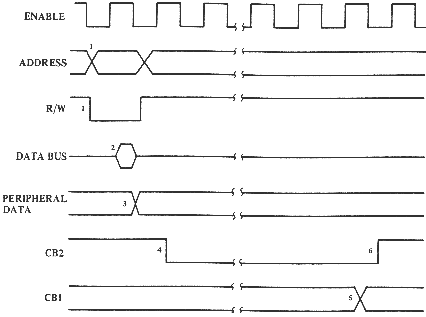 1. Processor puts out address of peripheral device and changes R/W
signal to write enable (low).
2. During phase two processor puts out data on Data Bus.
3. Data from the processor is accepted by the MCS6520 on the
falling edge of the enable clock.
4. Peripheral Interface device now begins the handshake by signaling the
peripheral device that data is available to read on the output port.
5. When the external peripheral device reads the data on the output
port it will respond by a change in CB1.
6. This change in CB1 is followed by a positive transition of CB2
signalling the processor that data was accepted.
Write handshake Sequence
FIGURE 2.6
-97-
1. Processor puts out address of peripheral device and changes R/W
signal to write enable (low).
2. During phase two processor puts out data on Data Bus.
3. Data from the processor is accepted by the MCS6520 on the
falling edge of the enable clock.
4. Peripheral Interface device now begins the handshake by signaling the
peripheral device that data is available to read on the output port.
5. When the external peripheral device reads the data on the output
port it will respond by a change in CB1.
6. This change in CB1 is followed by a positive transition of CB2
signalling the processor that data was accepted.
Write handshake Sequence
FIGURE 2.6
-97-
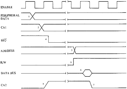
2.3 CONFIGURING THE INTERFACE BETWEEN THE MICROPROCESSOR AND THE SUPPORT CHIPS. The system block diagram (Figure 2.8) shows the basic data paths which al- low the MCS6500 system to operate. Data Bus, Address Bus, R/W signal, etc. are shown as simple connections between the various chips in the system. Although these data paths will exist in any system, no matter how complex, each element of the microprocessor interface must be examined to assure that each chip is properly driven with signals which meet all specifications for the device, to assure that the inter-chip timing is proper and to assure that the overall sys- tem is operating as required. 2.3.1 Assignment of Addresses in the MCS6500 System The only method which the microprocessor has for selecting between the various RAMs, ROMs, etc. in a system is through the address output lines. For this reason, the designer must use these lines very carefully to achieve minimum system cost and to assure satisfactory system perfor- mance. Before looking at how the address lines can be configured to minimize total system cost or program execution time, the designer should understand how the binary value associated with each address line is related to the total address space available to the microprocessor and how the AND func- tion of various address lines can be used to select large blocks of ad- dresses. Figure 2.9 illustrates the state of the three high-order address lines for the entire address space available to the MCS650X. Note that the highest order address line is a logic 1 for exactly half of the available address. The AND function of the two highest order address lines is a logic 1 for one-fourth of the available addresses, and so forth. Figure 2.9 also illustrates several AND functions derived from the three highest order address lines. Each is true for a different block of the available ad- dresses. Generation of the AND function of various high order address lines is extremely important because of the chip select techniques employed on the processor support chips. As described in Chapter 1, Section 1.5.2.4, the MCS6520 has three chip-select lines. The entire chip is selected for reading or writing data when CS1 and CS2 are high (> 2.4v) and CS3 is low
-99-
 Organization of Microcomputer System
FIGURE 2.8
-100-
Organization of Microcomputer System
FIGURE 2.8
-100-
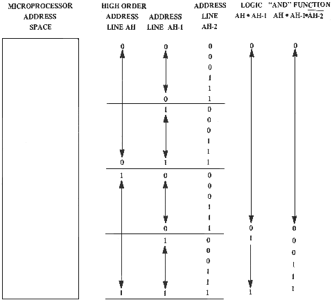 Example of 'AND" Function Using High Order Address Lines
FIGURE 2.9
-101-
Example of 'AND" Function Using High Order Address Lines
FIGURE 2.9
-101-
(< 0.4V). Selection of the address lines which enable the various chips in the system is a very basic but very important part of the system con- figuration task. It is important to note here that very few microprocessor-based sys- tems actually require that the processors be able to access a full 65,536 words. In fact, most systems can be programmed in less than 2,000 words for program and data memory. The full address space is made available pri- marily because it allows the configuration of systems with an absolute minimum of separate decoding chips between the processor and the support chips. It is possible to assign any block of address to each type of chip (RAM, ROM, peripheral interface chips, etc.) in the system. However, each of the assigned addresses must be mutually exclusive. Only one of the sup- port chips should be selected for every address used in the system program. 2.3.1.1 ROM Address Assignment The assignment of ROM addresses is dictated by the fact that the interrupt and RESET vectors must be located in the 6 high-order words in memory. These are fixed vectors and must be stored permanently in these locations. For this reason, the program memory (usually ROM) is usually assigned the high order addresses. In fact, the recommended procedure is to use A15 (A12 for MCS6504 and A11 for MCS6503 and MCS6505) to select program ROM. 2.3.1.2 RAM Address Assignment There are several factors which determine the location of the RAM in an MCS650X-based system. Data stored in memory under control of the in- ternal processor Stack Pointer will always go into Page One (ADH = 01). Also, the entire set of Page Zero addressing modes relies on there being data storage RAM in Page Zero. For this reason, the RAM in a MCS650X-based system should be placed in the low order addresses in memory. With the RAM in low order memory and the ROM in high order memory, the peripheral interface devices must go somewhere in between. This is accomplished in Figure 2.10 by using A15 x A14 to select ROMs, A15 to select RAM, and A15 . A14 to select all peripheral interface devices. This allows dif- ferentiation between the types of support chips. The addressing structure can be completed by allowing for selection of each chip in the groups.
-102-
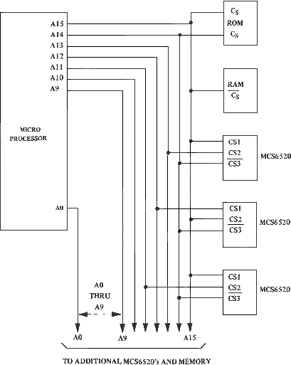 Typical Address Assignments
FIGURE 2.10
-103-
Typical Address Assignments
FIGURE 2.10
-103-
The addresses which select the various registers, peripheral ports, etc. within the peripheral interface devices normally used will not be sequential. For this reason, it is normally recommended that the tech- nique shown in Figure 2.10 be used to differentiate between the peripheral interface chips. This allows selection of 12 devices with no decoding in a MCS6501- or MCS6502-based system, up to nine MCS6520 devices in a MCS6504- based system, and up to eight devices in a MCS6503 and MCS6505-based system. 2.3.2 Additional Address Assignment Techniques In many systems, the techniques illustrated above may not represent the best solution to the system problem. This is particularly true if pro- gram execution speed is a primary consideration. The time required to access the peripheral devices can be reduced by putting these devices in Page Zero. The entire set of Page Zero addressing modes can then be used to access these devices. In addition, the polling of the MCS6520 control registers during interrupt servicing can be facilitated greatly by putting the control registers in sequential addresses. These registers can then be accessed using the Page Zero, Indexed addressing mode described in the Pro- gramming Manual. The address interconnect which allows this is shown in Figure 2.11. Note that this implementation requires external address de- coding chips but for the system requiring it, this incremental cost will result in higher operating speeds. The system designer must become familiar with the addressing lines and their effect on the address space available to the processor. Even more important, there is a significant relationship between software and hardware in microprocessor systems and a full understanding of both can allow optimization of the trade-off between speed and cost for the system under design. 2.3.3 Interrupts The basic concept of interrupts is introduced in Chapter 1, Section 1.3.2 of this manual. However, little is said there about the hardware and software techniques which are required to assure proper implementation of
-104-
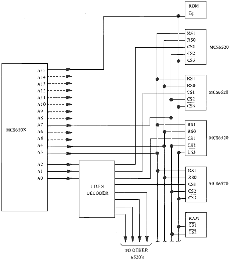 Page Zero Chip Select Addressing Scheme
FIGURE 2.11
-105-
Page Zero Chip Select Addressing Scheme
FIGURE 2.11
-105-
the interrupt system. This section is designed to introduce the designer to the details of interrupts and interrupt servicing techniques. 2.3.3.1 Interrupt Prioritizing Chapter 1 makes reference to various techniques for hardware prioritizing of interrupts to allow more rapid servicing of interrupts. The goal of this hardware is to allow the processor to go directly to the program which services the highest priority active interrupt without taking the time to poll each interrupting device. All hardware prioritizing techniques are based on the "priority encoder" shown in Figure 2.12. This device has eight inputs which are assigned a priority level from one to eight and generates a three-bit bi- nary code corresponding to the highest priority active input signal. The generation of this three-bit code is in reality a trivial task for the designer. However, relating this code to the address of the corre- sponding interrupt service routine is much more difficult and represents an opportunity for creativity on the part of the designer. Several solutions will be illustrated here to demonstrate what can be done. These are cer- tainly not assumed to be the only solutions. Each system must be considered separately to assure that the implementation chosen is as close to optimum as possible. 2.3.3.2 Example 1: Selecting the Interrupt Vector The final step of interrupt response within the processor is the fetching of an interrupt vector from two fixed addresses in memory. The interrupt vector located in these fixed addresses identifies the address of the software which the processor executes to poll the interrupting devices. Instead of pointing to the polling routine, it would be much faster to go directly to the software which actually services the interrupt. This re- quires a unique vector for each interrupt. The technique illustrated in Figure 2.12 assumes that the inter- rupt vectors are located in ROM at addresses below that normally assigned to the interrupt vector. The decoder detects the fact that the processor is reading FFFE or FFFF. At this time the address inputs AD1, AD2 and AD3 into the ROM are driven from the priority encoder. Instead of accessing FFFE or FFFF, the interrupt vector will come from two addresses selected by
-106-
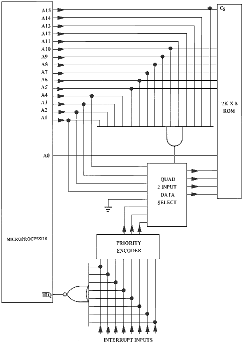 Selecting the Interrupt Vector
FIGURE 2.12
-107-
Selecting the Interrupt Vector
FIGURE 2.12
-107-
the priority encoder. The actual hardware involved is quite simple and the interrupt response time is an absolute minimum. 2.3.3.3 Example 2: Using the Processor Software Power These several solutions to the vectored interrupt problem take ad- vantage of certain instructions which can be performed by the processor. The first of these uses an instruction called the Jump Indirect. This in- struction causes the processor to begin executing the program located at that address contained in two sequential memory locations. As in Example 1, the three-bit output from the priority encoder becomes part of the address of the interrupt software. If the output of the priority encoder is connected to the inputs of a peripheral interface device, the processor can then perform a Jump Indirect operation using the address on the two peripheral I/O ports. This is shown in Figure 2.13. Another solution which takes advantage of the processor software is shown In Figure 2.14. Once again the output of the priority encoder is connected to the inputs of a peripheral I/O port. However, in this ap- proach, the priority encoder is connected to the low order bits and the other bits can be used as control or input lines for other functions. In this method, the three bits from the priority encoder will be- come part of an address established in memory. This address will then be used in a Jump Indirect instruction as before. This operation is detailed in Figure 2.15. 2.3.4 The Application of RDY to Controlling the Memory Interface The ability to stop the microprocessor can be extremely important when using memory devices which are not directly compatible with the MCS650X family. The RDY line on the MCS6501, MCS6502 and MCS6505 can be used to stop the processor in any "non write" cycle, i.e., any cycle in which the pro- cessor is not attempting to write data into memory. The processor can be stopped for any number of clock cycles, from one cycle for interfacing with slow memories to many cycles for DMA applications and for single cycle exe- cution. 2.3.4.1 Interfacing Slow PROMs One of the principal applications of ROY is in the control of light-erasable PROMs or EAROMs. These devices generally have longer access
-108-
 Priority Encoder Connected to Low Order Bits ofMCS6520
FIGURE 2.14a
-110-
Priority Encoder Connected to Low Order Bits ofMCS6520
FIGURE 2.14a
-110-
 Priority Encoder to Peripheral Interface Scheme
FIGURE 2.14 b
Priority Encoder to Peripheral Interface Scheme
FIGURE 2.14 b
Software Program to Implement Interrupt from above Hardware Configuration FIGURE 2.15 -111-
times than that required by the microprocessor when operation at 1 MHz clock frequency and are incapable of making data available on the data bus within 100 nanoseconds of the end of the Phase Two clock pulse. The Phase Two clock pulse is used to latch data or instructions on the data bus; therefore, if the data is not available at the correct time, the processor must be held up for one full cycle. The instruction will then be latched on the following Phase Two pulse. Execution of the instruction will then proceed during the next cycle. Suggested logic for performing this func- tion is shown in Figure 2.16. Note that the data present on the data bus during the Ø2 clock pulse after ROY goes high is the data that will be used in the instruction execution which takes place during the following cycle. 2.3.4.2 Direct Memory Address (DMA) Techniques Transfer of data from peripheral storage devices into the micro- computer data memory (RAM) can normally be handled one byte at a time under control of the microprocessor. However, in large data terminals, control systems, etc. the primary data storage device may he a high-speed tape or disk. In systems such as these, the data transfer from the storage device into memory must be performed at speeds greater than the processor can handle. The control of the transfer must be performed outside of the pro- cessor in a separate controller and the peripheral device must gain direct access to the system RAM. Direct Memory Access requires primarily that the processor have no need to access the memory involved. This is generally assured by stopping the processor completely. The DMA controller must then gain access to the R/W line and both the address and data busses on the memory unit. Provision for stopping the processor is available on the MCS6501, MCS6502 and MCS6505. This is accomplished by pulling the ROY line on the processor to GND (< 0.4V). The processor will stop in the first non-write cycle with the data bus in the high-impedance state. After the processor has stopped, the DMA controller must provide the address and data for the memory and must control R/W if data is being transferred into memory. Providing addresses for the memories can be accomplished by gating addresses from either the DMA controller or the microprocessor into the memories. This can be accomplished very easily with a Quad 2-input data
-112-
selector. During the DMA operation, the addresses fed to the memories are those generated by the DMA controller. After the DMA operation is complete, the input select signal to the data selector is inverted and the addresses generated by the processor once again determine which memory word is being accessed. The R/W line to the memories can be controlled in the same way as the address lines. The data bus must be controlled in a somewhat different manner. This is necessitated by the fact that these lines are "bi-directional"; the data bus pins on the processor and the support chips act as both an input and an output. The output buffers in each of these chips are capable of entering a high impedance state to allow any of the devices to drive the bus during data and instruction transfers. For this reason, a bi-direc- tional, "three-state" bus extender is required to interface the DMA con- troller to the system data bus. The logic necessary to provide full address bus and data bus control for DMA applications is shown in Figure 2.17. The MCS6501 provides a Bus Available output to signal the DMA con- troller that the processor has stopped and that the DMA controller can pro- ceed to access memory for reading and writing data. This signal will go high during the Phase Two clock in the first Read cycle (R/W = 1) which follows RDY going low. This will occur immediately if RDY is pulled to GND (< 0.4V) during a Read cycle. The discussion of the processors in Section 1 describes this in detail. The MCS6502, MCS6503, MCS6504 and MCS6505 do not make available the Bus Available signal. However, these processors still stop in the first non-write cycle. For this reason, the logic shown in Figure 2.17 should be used to generate a Bus Available signal for the DMA controller. 2.3.4.3 Control of Dynamic RAMs in the MCS6500 System For systems which must contain a large quantity of Read/Write memory (RAM), the 4096-bit dynamic RAMs can provide the required storage with a minimum number of parts. Currently available dynamic RAMs are cap- able of storing four times as much data as similar static devices. How- ever, there is one major drawback to these devices--they must be refreshed periodically. For most devices currently available, this refresh period is about 2 milliseconds for the entire chip. Refreshing the entire chip
-113-
-115- Interfacing Scheme for Slow PROMs
FIGURE 2.16
Interfacing Scheme for Slow PROMs
FIGURE 2.16
 Logic Used to Generate Bus Available Signal for DMA Applications
FIGURE 2.17
-114-
Logic Used to Generate Bus Available Signal for DMA Applications
FIGURE 2.17
-114-
requires 32 Read operations which can be performed all at once every 2
milliseconds, or 1 approximately every 64 microseconds.
Unless a separate controller is used to perform this refresh
operation, the use of dynamic memories can be very detrimental to system
performance.
As with any Direct Memory Access, the processor must be stopped to
assure that the processor and the DMA controller are not attempting to
access the memories concurrently. The ROY input provides this capability.
A counter operating directly from the system clock will provide a very con-
venient refresh signal. Each time the counter goes through a count of 63,
a "refresh request" pulse is generated. The actual memory refresh opera-
tion must take place during a Read operation with the processor stopped for
1 cycle. Determining when the processor has stopped is exactly the same
problem as in DMA operations. The MCS6501 will generate a Bus Available
pulse when the processor has stopped. In the other processors, the control-
ler must pull the RDY line low and must then examine the R/W line to deter-
mine when the processor is in a Read cycle.
The specific operation performed during the refresh cycle is a
function of the devices being used. However, it should be noted the time
available for refreshing the memory is "N - 1/2" cycles, where N is the
number of cycles that the processor is stopped. This formula is based on
the fact that the first half cycle is lost due to the fact that BA does not
go high until Ø2 in the MCS6501 and that the state of the R/W line cannot
be considered valid until Ø2. Control of the memory address lines must be
returned to the processor at the beginning of Ø1 if the memories are to
have a full cycle to make valid data available on the data bus. This leaves
one-half cycle available to perform the refresh operation if the processor
is stopped for one cycle. A full 1-1/2 cycles can be made available by
stopping the processor for two cycles. This latter implementation is more
compatible with most dynamic RAMs currently available.
As described above, a primary problem in the implementation of
dynamic RAM systems is knowing when the processor has stopped. A full one-
half cycle is required in the implementations described above. The MCS6502,
however, provides a signal which can be used to predict that the processor
will stop in the very next cycle. This is the SYNC signal. It is impossible
for a Write operation to immediately follow an instruction fetch cycle.
This allows the memory refresh controller to assume control of the address
lines at the beginning of that cycle instead of after the trailing edge of
Ø1.
The RDY line is pulled low on Ø1 and the processor is guaranteed
to stop. Control of the address lines is returned to the processor on the
next Ø1 and RDY is set high at the same time. The result is the refresh
logic had a full 1 cycle to refresh the memories and the processor lost only
1 cycle of execution time. A suggested configuration for this control logic
is shown in Figure 2.18.
 Control Logic for Refresh Signal for Dynamic RAMS
FIGURE 2.18
-116-
Control Logic for Refresh Signal for Dynamic RAMS
FIGURE 2.18
-116-
2.3.5 Hold-Time Control--MCS6501
The data bus hold time required by the MCS6500 family parts is de-
fined in Chapter 1. Each chip in the system requires that the data on the
data bus be held for 10 nanoseconds past the trailing edge of the Phase Two
clock pulse. Also, each device is guaranteed to hold data for this length
of time to assure proper operation of the other devices in the system.
This only assures that the family parts will work together. Operating with
other RAMs and peripheral devices requires that a careful study be made of
the timing requirements. This section discusses techniques for properly
interfacing RAMs which require more than 10 ns hold time guaranteed by the
processor. These techniques are applicable primarily to the MCS6501 since
this device uses the input clocks and the DBE input.
The data which is to he written into memory is actually available on
the inputs to the processor data bus buffers from the beginning of the Phase
One clock pulse. This data is normally gated onto the bus during Phase Two.
However, if greater hold time is required, the designer can take advantage
of the fact that this data can really be gated out during Phase One. This
requires that a delay be provided between the Phase Two and Phase One clock
pulses. The DBE output can then be connected to a Phase One pulse to cause
the data to remain on the bus past Phase Two pulse which is used to latch
data in memory. This timing is shown in Figure 2.19.
-117-
 Timing Analysis of Data Hold Time
FIGURE 2.19
-118-
Timing Analysis of Data Hold Time
FIGURE 2.19
-118-
2.4 ADDITIONAL SYSTEM CONSIDERATIONS After the basic system configuration is complete, extensive breadboarding and testing is usually required before the design is finalized. However, this breadboarding and evaluation must be preceded by a complete evaluation of the cost and performance of the proposed design to assure that the various goals of the project will be met. The first step in evaluating the design is to estimate the amount of ROM and RAM which will be required and to estimate the number and type of interface devices required to control the peripherals 2.4.1 Peripheral Interface Devices The number and type of peripheral devices can generally be estimated very accurately. However, it is important to keep in mind that these esti- mates must be subject to review after a full analysis of system performance is completed. The designer may find it necessary to use a special-purpose interface part or to redesign the I/O structure if the evaluation of system performance reveals that the system cannot operate at the required speed. Use of special-purpose peripheral interface parts will reduce the number of tasks which must be handled by the processor and consequently can increase the overall system speed, but this generally involves additional component cost. Likewise, the use of a fully vectored interrupt can lead to increased performance at increased cost. The goal of any design program must be to meet all the system performance at the minimum possible cost. After the various peripheral devices in the system have been evalu- ated to determine the number of inputs and outputs required, the total re- quired by all peripherals can be divided by 16 to determine the number of devices required. This is a good first approximation which will be re- evaluated as the system development progresses. 2.4.2 RAM The evaluation of the amount of RAM required by the system is a some- what more difficult problem than estimation of peripheral devices. This is due primarily to the fact that much of the RAM is required by the system software as working storage, such as storage of immediate results in
-119-
arithmetic operations. Since the system program will probably not be written when these estimates are first attempted, the probability of error in this portion of the estimate may be fairly high. In addition to working storage, the RAM must provide storage for: 1. The Stack; this is described in the Programming Manual. 2. Peripheral input data storage. 3. Peripheral output data storage. Items 2 and 3 above can be evaluated quite accurately since a de- tailed analysis of the peripheral devices has usually been completed when these estimates are first attempted. In general, a block of RAM must be made available for each peripheral device. The amount of RAM required for each is a function of the type of peripheral device being interfaced and just how the device is to be controlled. The amount of RAM required by the stack is a function of both the interrupt structure and the system software. As a result, an estimate of this requirement must be based on the system programmer's best estimates of his requirements. This should be combined with an estimate of the re- quired working storage and the peripheral data storage requirements to ob- tain an estimate of the total system RAM. 2.4.3 ROM The amount of ROM required in a system cannot be determined accu- rately until the system program is completed. However, by partitioning the system program into definable pieces, an estimate can be made of each task and the total can be obtained of the ROM required by each section. Most programs consist of easily defined sections such as the software for each peripheral device, arithmetic routines, etc. These are the pieces which should be examined separately to estimate the ROM required by each.
-120-
2.5 EVALUATING SYSTEM PERFORMANCE As discussed in the previous section, the peripheral interface structure for a system is fairly easy to configure if one assumes that MCS6520-type de- vices are used. However, before going too far into hardware construction, it is important that the total system performance be evaluated to minimize the proba- bility that major problems will arise in the later stages of the design. Evaluating system performance involves first determining whether or not the processor is capable of processing all interrupts with the speed required and then determining that the processor has sufficient time to perform non- interrupt operations. The prioritized interrupt structure assumes that at times, more than one interrupt will occur and that there will be delays encountered in servicing some interrupts caused by the presence of other interrupts. This structure will per- form satisfactorilv if these delays are not too great. The interrupt processing time should be evaluated starting with the highest priority interrupt, then going to the next highest priority, each time keeping in mind the total time which can be lost due to concurrent higher priority interrupts. Each time an interrupt is examined, the worst microprocessor re- sponse time which can be encountered should be estimated. If this time is still adequate for the function being handled by the interrupt, that aspect of the system operation can he expected to perform satisfactorily. The ability of the MCS650X microprocessors to handle interrupts quickly and conveniently represents one of the real strengths of this microprocessor family. However, in any system being developed, it is important that the percentage of processor time spent servicing interrupts not be so large that the internal data handling, arithmetic operations, etc. cannot be executed properly. Since the interrupts are usually asynchronous and are not related directly to the main line program, the time lost to interrupts can usually be viewed as an average percentage of the total time. The speed with which the main program can be executed will be reduced by this percentage. The interrupt service routines are usually short and easy to evaluate. However, the main program is much more difficult to estimate. Fortunately, it is also usually much less critical. Those operations which must meet a
-121-
particular speed requirement can be examined in detail by the programmer to de- termine the execution time. This estimated execution time must then be reduced to allow for the time lost to interrupts. The final step to assuring satisfactory system performance is a worst-case analysis. This is to determine if there are any places in the program where worst-case interrupts can cause excessive delays in the execution of other pro- grams being executed. Although the effort involved in a complete worst-case analysis is usually excessive, this is one part of the system development task which con lead to significantly greater assurance of success for the entire de- velopment process.
-122-
CHAPTER 3 BRINGING UP THE MCS6500 MICROCOMPUTER SYSTEM
3.0 INTRODUCTION TO MICROCOMPUTER TESTING After many hours of planning, hardware construction, and programming effort, the microcomputer system designer must face what can be his most difficult task: "bringing up" his system. The modern microcomputer with its minimum chip count, and its minimum number of control and data lines represents a tremendous advance in system design when everything is working properly. However, it can also repre- sent a testing nightmare to the designer who is attempting to trouble-shoot the hardware and software which constitute the total design. A microcomputer lacks many of the things which make testing of conventional logic relatively convenient. To begin with, one simply cannot see most of the control signals, data transfers, etc. which allow the system to operate. In addition, it is impossible to examine directly the contents of the registers and latches which store data within the processor. This data can only be examined indirectly by looking at the signals on the inputs and outputs to the chip at the proper time. This problem is compounded by the fact that many programs must be tested "dynamically"; i.e., the system must be running at its full operating speed with non-recurring events or with a total lack of usable oscilloscope triggering signals. For these and many other reasons, it is important that the system designer build effective testing capability into both his hardware and his software. This is particularly true for the pre-production prototypes. When combined with the procedures discussed below, this will minimize both the time and the effort spent in producing that first operational system. After the program and the hardware are completely debugged, many of the testing tools discussed below can be removed from the prototype design without affecting system performance. This allows the designer to arrive at his final production design very shortly after he has proven that the prototypes are operating satisfactorily.-123-
3.1 STATIC TESTING 3.1.1 Introduction Static testing, i.e., execution of the program, one cycle or one instruction at a time, is the first step in the checkout of any system. In this way, the general flow of the program can be examined and for much of the program the validity of data transfers into and out of memory can be verified. As shown in Figure 3.1, the logic necessary to control RDY to allow Single Cycle and Single Instruction Execution is relatively simple. This hardware and its use in system testing are discussed below. 3.1.2 Single Cycle Execution The timing required for Single Cycle Execution is shown in Figure 3.2. In this operation, the RDY line has been brought low (GND) to halt the processor. To allow execution of a single cycle, the RDY line goes high (+2.4v), for one cycle each time the Single Cycle switch is acti- vated. Note that the RDY line goes high while the Ø1 clock is high and the internal timing counter advances on the next Ø1 clock pulse. Single cycle operation allows stopping the processor in any cycle except a WRITE cycle. This allows detailed examination of all cycles of the instruction fetch operation. In addition, it permits detailed examina- tion of operand fetches. Thus, it is possible to verify the operation of most of the hardware involved in memory addressing and control. It is also possible to verify the operation of most of the peripheral interface hard- ware. This can greatly reduce the time required to test the full dynamic operation of the peripheral device. Note that if depressing the Single Cycle switch allows the processor to advance into a WRITE cycle, the processor will complete this cycle and will then stop in the first READ cycle (R/W = 1) which follows. This tim- ing is shown in Figure 3.2. Appendix A contains a detailed summary of the data which should appear on the address and data lines during each cycle of the MCS6501 and MCS6502 instructions. Note that the processor often puts out an address and fetches data which it ignores. This is an inherent feature of the processor which uses a "look ahead" approach to pipelining. Examination of the SYNC signal will allow the designer to keep track of exactly when the data fetched from memory is utilized within the processor and when it is ignored.
-124-
 Suggested Static Test Control Logic
FIGURE 3.1
-125-
Suggested Static Test Control Logic
FIGURE 3.1
-125-
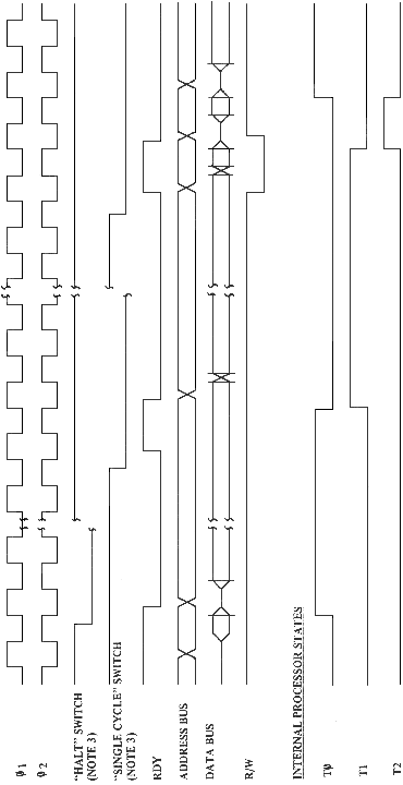
A very simple "data trap" can be built into prototype systems to allow examination of the address and data generated by the processor during WRITE cycles. This trap may latch the contents of both the address and data busses or it may latch only the address bus. The latter can be suf- ficient if a separate means of examining data in memory is provided (see Section 3.3). A suggested configuration for the "data trap" is shown in Figure 3.3. This circuit can be used to display the contents of the ad- dress and data busses for both READ and WRITE cycles. The WRITE data is latched and held during the next READ cycle. Depressing the Latch Reset switch then opens the inputs to the latches and allows monitoring of the subsequent READ cycles. 3.1.3 Single Instruction Execution While it is extremely useful to be able to analyze the execution of each instruction in detail, it is often sufficient just to look at the gen- eral program flow. This is particularly useful when examining the opera- tion of branches and jumps in a program. Single instruction execution is designed to allow this capability on the MCS6502 which outputs a SYNC sig- nal. The operation of the single instruction execution logic is based on generation of a SYNC signal within the processor. This signal goes high (> +2.4v DC) during each OP CODE fetch cycle. Single instruction execu- tion is implemented by using SYNC to force RDY low (< +0.4v DC). Under these conditions, the processor will always stop with an OP CODE address on the address bus and the OP CODE on the data bus. The timing for this operation is shown in Figure 3.4. Note that this diagram assumes that the processor is stopped in an OP CODE fetch cycle. Depressing the Single Instruction switch (Figure 3.1) allows execution of that instruction. The processor then stops when the next OP CODE is fetched.
-127-
 Microprocessor Single Cycle Data Trap
FIGURE 3.3
-128-
Microprocessor Single Cycle Data Trap
FIGURE 3.3
-128-
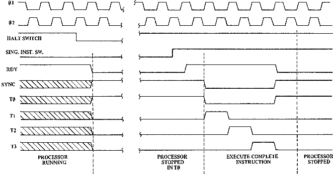 Single Instruction Execution
FIGURE 3.4
-129-
Single Instruction Execution
FIGURE 3.4
-129-
3.2 DYNAMIC TESTING 3.2.1 Introduction Through static testing techniques, the designer should be able to verify the operation of most of his processor interface hardware, such as the Bus Expanders and Address Decoders (for selecting ROMs, RAMs, etc.). However, this is only a first step to assuring proper system operation. Most peripheral devices cannot be properly tested unless the processor is operating at full speed. This necessitates full dynamic testing. Dynamic testing generally involves causing the processor to execute a program loop, i.e., to execute a repetitive sequence of instructions. This allows the use of an oscilloscope in examining the processor opera- tion. This repetitive operation can be externally induced through the RES or Interrupt (IRQ or NMI) lines, or it can be a part of the program being executed. Both techniques play an important role in the system checkout process. 3.2.2 Externally Induced Loops The most direct means of causing the processor to execute a loop is to drive one of the direct inputs (RES, IRQ or NMI) with a signal gen- erator. This technique can be used to trouble-shoot systems which are only partially operational since it does not rely on proper execution of a par- ticular set of instructions to cause looping to occur. However, this tech- nique can only be used if an oscilloscope can be employed in examining system operation. To do so requires an effective scope-synchronizing signal. For this reason, the following section will discuss not only the signals to be tested and the waveforms which one should see but also the techniques one may use to assure generation of an effective scope sync. Probably the most basic operation performed within the processor is the RESET function. Without the RESET hardware and software operating pro- perly, the system will never enter its normal operating mode. For this reason, the first major function to be tested, both statically and dynam- ically, is the RES input. A suggested configuration for dynamically testing the RESET input is shown in Figure 3.5. In this diagram, the RESET input is being driven from a signal generator. Between the signal generator and the processor is a D- type flip-flop to synchronize the chip reset signal to the processor clocks.
-130-
 Suggested Configuration
For Dynamic Reset Testing.
FIGURE 3.5
-131-
Suggested Configuration
For Dynamic Reset Testing.
FIGURE 3.5
-131-
This synchronizing is extremely important because it stabilizes the data being displayed on the oscilloscope with respect to the scope sync. The most effective procedure for testing the dynamic operation of the RESET function is to reset the system initially at a rate of approxi- mately one-fifth of the clock rate. This will allow the processor to execute the first few instructions in the reset sequence before being re- cycled. The designer can then closely examine the timing of address, data and R/W signals. Use of the delayed sweep feature available on most modern oscilloscopes will allow examination of any part of the RESET operation. When proper operation of the RESET input has been verified, the same technique can be applied to both the IRQ and the NMI inputs. Driving either of these inputs with a signal generator synchronized to the processor clocks will allow a close examination of the dynamic operation of the interrupt polling sequence. This provides a very important look at the Peripheral Interface selection logic to assure that all peripheral devices are respond- ing to the proper address. 3.2.3 Software Loops During system checkout, the designer must verify the operation of many simple functions which must all operate properly before the entire sys- tem is operational. The use of simple software loops will allow a detailed examination of one function at a time. Most importantly, it allows the designer to use an oscilloscope to examine events which may occur very in- frequently and which are normally very difficult to see. The execution of software loop requires the writing of a program which ends in a JMP back to the beginning of the program. Once the processor enters the loop it will continue to execute the same sequence of instructions until the RESET switch is pushed. To utilize software loops effectively there must be an event which happens only once each time the processor executes the loop. This signal can be used to trigger the oscilloscope. Including a single WRITE operation in the program allows the R/W signal to be used to trigger the scope. Like- wise, careful selection of address in the program will allow use of an address line as a scope sync. Finally, lacking anything else, setting and resetting a peripheral interface device output pin at the beginning of the program provides a very effective sync signal.
-132-
3.3 SYSTEM DIAGNOSIS USING HARDWARE PROGRAMMER AIDS In addition to the techniques described in which the user utilizes oscil- loscopes and his own innovative techniques for analyzing data, MOS Technology, Inc. makes available to the user several hardware aids which assist in debugging of a microcomputer system and also a software aid called the emulator. The hardware aids are a Keyboard Input Monitor (KIM), a Teletype Input Monitor (TIM), and a Microcomputer Development Terminal (MDT) . Each of these aids is designed to allow the debugging of microprocessor code without need to resort to scopes or other data trapping techniques, but rather attempts to reduce the problem of debugging the code to the same techniques that are available on a large computer system. The basic assumption of each of these devices, either hardware or software, is that the microprocessor system is connected correctly, all the electrical characteristics have already been checked and met and that the only problem to be solved is one of debugging programs and I/O hardware which have been entered into the microcomputer. Each of the hardware techniques assumes that the user will start his design sequence with all of his programming being done in some form of random access memory which is loadable from an I/O device, examinable by the I/O device and changeable by the I/O device. This is the normal first step in developing a microcomputer system and one that should be used prior to committing any of the hardware to PROMs or alterable memory. The only exception to this is if the user is taking advantage of the software emulator and if his program is such that the emulator can give him a significant degree of confidence in his coding in which case the use of the KIM or TIM devices is primarily that of allowing him to have final debugging access to his various memory locations. Therefore, the common characteristic of all these approaches is that by some technique, in the case of the Emulator by reading an input file, in the case of TIM by reading in an input tape from the output Cross-Assembler, in the case of KIM loading a program into memory by hand, and in the case of MDT either assembling the pro- gram or loading input data from the Cross-Assembler, the program has been entered into a program storage. Each of these techniques allows the user to
-133-
initialize various memory and register locations and to "start execution" of this program at a memory location. Techniques are implemented which allow the user to stop his program at a particular point and analyze the results of the opera- tions which have just been completed. If the results are correct, the coding between the start point and the stop point is correct. If the coding is incor- rect, the user analyzes the data which he displays by use of the I/O device and the hardware or software that interfaces it, and determines by inspection of the data and analysis of his coding what error could cause the results detected. If the technique of just analyzing coding is not sufficient, each of these systems has the ability to allow the user to go in and re-execute the code with new data or the original data, only stopping at earlier stop points until he is able to trap the operation that causes the erroneous data to occur. Both the emulator and MDT have additional features which allow the user to analyze the operation of instructions as they occur which is very useful in determining which part of the program causes operations to be performed incorrectly. The normal design cycle should actually include a combination of techniques. If the user is not using MDT, then he should write his code on a Cross-Assembler and debug much of his loops and non-I/O programming using the Emulator. The Emulator has been designed to allow very easy analysis of data paths, loops and performance of program on a non-hardware basis. It is particularly useful for the user who is developing routines which have significant loop and subroutining or any completed algorithm. The use of emulation has the following advantages: 1. It gives the power of a large machine to allow tracing operations which are not very feasible at the hardware level. 2. It may indicate prior to the time that the hardware is committed that more memory or more time is required to perform an operation which may dramatically change the hardware implementation which is to be committed. In any case, attempting to bring up the microprocessor system without use of assemblers and an interface module such as TIM is not the most efficient use of the designer's time. For the user who is just starting in microprocessors, the KIM technique is acceptable because the length and complexibility of the programs to be written should be shorter and the user can program directly in Hex and debug using the KIM exclusively.
-134-
3.3.1 KIM--Keyboard Input Monitor KIM allows the user to key in Hex values into specified memory loca- tions and to monitor results. KIM is available to the system designer in several forms. In its simplest form, a single device of the MCS6530 type including 1024 bytes of pre-programmed ROM may be included as a component in an existing system. The KIM array includes a monitor program which provides the following features: a) Data input and output control from serial teletypewriters (ASR 33, Silent 700, etc.) b) Data input and system control from a 22-key keyboard c) Address and data display on a 6-digit, 7-segment type display. A microprocessor system designed to include the KIM array will allow the designer to perform the following operations: a) The user may select keyboard (KB) or teletypewriter (TTY) mode for entry, display and control. b) If in KB mode, the user may enter address or data fields from the keyboard. The user may display the contents of any address location in the system and can modify the contents of any address location (other than pre- programmed ROM locations). The step operation (STEP key) provides a con- venient method for displaying the data contained in successive memory loca- tions. Program execution may be authorized to begin from any selected starting address using the RUN key. c) If in the TTY mode, the user may obtain a printing of the data at any memory location. He can modify the data contained in any memory loca- tion. Program listing from any start address to any end address may be authorized. Paper tapes may be loaded or generated automatically. Finally, program execution may be initiated from any selected starting address. d) In either mode, the user terminates program execution using the STOP key which will return control of the system to the KIM program. Alternatively, a depression of the RST key causes a total reset of the sys- tem and a return of the system to KIM program control. The KIM array is also available to the system designer as a part of a special design-in sub-system provided in the form of a printed circuit card. Included on this card are the following functional elements:
-135-
a) MCS6502 microprocessor array b) MCS6530-002 array (containing the KIM monitor program) c) 22-key keyboard and mode-select switch d) 6-digit, 7-segment LED display e) 1024 X 8 RAM f) mcs6530-003 array providing an interval timer, 16 I/O pins, and 64 bytes of RAM g) All interface circuits for operation with serial teletypewriters. This subsystem provides the same operating features described earlier but is supplied as an operating unit requiring the user to provide only the +5Volt power supply in order to commence operating. As a "stand- alone" subsystem, the user may enter and debug programs of up to 1024 steps and control the action of up to 16 I/O pins. For further details on physical and operating characteristics of the KIM array and subsystem, the reader is referred to the KIM manual supplied separately. 3.3.2 TIM - Teletype Input Monitor TIM is a preprogrammed MCS6530. The application of the Teletype Input Monitor is to allow the user to interface to an ASCII device such as a Teletype, CRT, Execuport, etc. using the ASCII serial communication tech- niques to communicate to and from the microprocessor. This effectively allows the user to load memory from the keyboard or from paper tape or cassette which are attached to his device. By the addition of a single TTL package to the system, TIM can be configured so that it is the starting point for the microprocessor, but once the initialization has been accom- plished it transfers itself out of the start-up memory, changes the rest of the microprossessor memory to normal configuration and operates trans- parent to the microprocessor. The technique for using the TIM to develop a microprocessor system is primarily after the system is determined to be wired correctly by the techniques already described. It is then used to debug the user's code by means of allowing the user to input pre-specified values, execute portions of the code and examine the results. It should be noted that because I/O devices are extension of memory debugging techniques are simplified. They can be configured to
-136-
control I/O devices to test that lights can be lit, switches tested, motors started and stopped, etc. For instance, all of the connections to lights and switches can be checked from the teletype keyboard by writing into the I/O registers the appropriate code that turns on the lights. Correct operation of switches can be checked without the program running by putting the switches in either state and reading the I/O device result indicated to the programmer. This type of checking totally shakes out the I/O connections to make sure the I/O device is located in the cor- rect memory address, determines that the wiring to the I/O devices is cor- rect and checks on the microprocessor bus. A rational technique for using either TIM or KIM is to interconnect the device into the system to get the microprocessor to pass the single- step start-up sequence and then to use the debugging capability of the TIM prior to executing any of the user's code to verify that all input/output connections are correct. In cases such as stopping motors and other devices which require timing, the proper connection to the motors and other devices can be checked without the motor itself physically being checked by uncon- necting leads, opening up connectors and verifying with a scope or a meter that the microprocessor's influence at that point is as would be expected on a static basis. Therefore, this technique is recommended as the second step of a start-up sequence. Significant details are given in the section on the use of restart or start sequence and a single cycle operation to verify the interconnec- tion of most of the system. It should be recalled that the instructions were given independent of the coding that was available to the programmer. The advantage of using the TIM or KIM in the start-up check-out is that there is known code which is guaranteed to be accurate that should be evoked during this start-up sequence. By looking at the coding of the ROM as it appears in the documentation on the TIM or KIM, the user can use the known sequences from the TIM or KIM program to verify the start-up sequence, thereby removing one more variable. Therefore, all initial systems check- out should be done using TIM or KIM program first in the start-up sequence to make sure that the interconnection to TIM and to memory are cor- rect. Then once the basic operation of TIM has been verified, there is a known sequence that the TIM will go through dynamically which will allow the user to verify that the TIM is operational. Then the user should
-137-
verify the rest of his memory and I/O connections by use of writing and reading in the memory locations using the debugging feature of the TIM or KIM. This verifies the connection and operation of each of the chips of the system and will verify all the interconnections to all outboard devices. Now the problem is truly reduced to making sure that the program- mer's code is correct and the user's program can be loaded by means of either through-the-keyboard or through-the-auxiliary devices. The program can be debugged as a program rather than worrying about whether or not the problem is one of hardware or software. By definition other than incorrect timing to I/O devices, the problem has been reduced to one of programming mistakes. For a more detailed discussion on the programming on TIM, the user is referred to the TIM manual supplied separately. 3.3.3 MDT--Microcomputer Development Terminal Almost all of the sections in this report had to do with how one goes about interconnecting a system and debugging it. MDT is a prepackaged system and, therefore, should not have the problems described above unless it is being used in circuit emulation mode. Therefore, the user will pri- marily be debugging his programs and his basic interconnection to his I/O devices with the MDT. Therefore, use of the MDT represents a significantly different technique than described in this manual. This technique is de- scribed in the MDT manual.
-138-
3.4 MICROPROCESSOR START-UP PROCEDURE 3.4.1 Introduction This section attempts to tie together all of the techniques previ- ously discussed into one ordered procedure. This procedure is based on experience gained in bringing up systems using processors from several different manufacturers. While it is certainly true that no single pro- cedure can be expected to catch all the software and hardware errors which can exist in microcomputer systems, it is hoped that this step-by-step approach will allow the designer to bring up his system with an absolute minimum of difficulty. This procedure assumes the existence of Single Cycle and/or Single Instruction logic. Any of the System Development tools discussed in Sec- tion 3.3 will assist the user in bringing up his system. These devices allow convenient entry of test programs as well as modification of the sys- tem program and data. Each step in the procedure includes the following information: * Section of the System hardware/software to be checked. * Hardware, test equipment, etc. required to perform the test. * Action to be taken in implementing the test. * Expected results. * Suggested procedures for analyzing failure modes. It cannot be emphasized too strongly that one must utilize a very methodical, step-by-step procedure aimed at solving one problem at a time within the system. It is very easy for several problems to amplify each other to such an extent that nothing within the system seems to be operat- ing properly. Correcting problems one at a time will ultimately yield a complete working system with minimum frustration. 3.4.2 System Power--Step 1 It is generally recommended that first prototypes of microcomputer systems be built using sockets for the ICs (processor, memories, etc.). One distinct advantage of this technique is that it allows the designer to verify that Vdd and Vss are properly connected to each socket before the chips are inserted. The Vdd line should be within the tolerances specified about the 5 volt nominal relative to Vss. This basic first step can help avoid power supply connections which may be fatal to the chips in the sys- tem.
-139-
After using a voltmeter or oscilloscope to check power connections, insert the processor into its socket and verify that the additional cur- rent drain is within specifications for this device. Before inserting the other devices, examine the address lines, SYNC line (6502) and the output clocks (6502, 6503) to make sure that the pro- cessor is generating signals. The address lines should be incrementing and the sync line should be generating regular, positive going pulses. The RES line and the RDY line should be high (> +2.4V) for this test. If the processor appears to be operating and power consumption is reasonable, the rest of the devices in the system can be inserted into their sockets. 3.4.3 Basic System Timing--Step 2 Before one can expect a microprocessor system to function, proper operation of the basic system timing signals (Ø1, Ø2, etc.) must be veri- fied. The most important of these signals is the system clock. A common fault in MC6800 and MCS6501 systems is generation of input clocks (Ø1 and Ø2) which are not full voltage or which have significant overlap. Another very serious difficulty often encountered is undershoot. Each of the specifications listed in the data sheet for the system clocks must be properly met. Figure 3.6a illustrates the problems often en- countered in clock signals such as undershoot and overlap. Figure 3.6b is an example of MCS6501 Ø1 and Ø2 clocks as they would normally appear in a properly operating system. In systems based on other than the MCS6501, the clocks which must be examined are the processor output clocks. In the 6502, both phases (Ø1 and Ø2) are available for driving the rest of the system. In this system it is necessary to check the clock timing very carefully to assure that the timing of the clock signals within the processor is compatible with that used on the support chips. Using an oscilloscope, compare the Ø1 input clock and the Ø2 clock presented to the support chips to verify that the delay due to clock buf- fering does not exceed the allowable maximum. 3.4.4 System Reset--Step 3 Static and dynamic analysis of the Reset function can provide very detailed information on how the system is operating. In fact, it is this
-140-
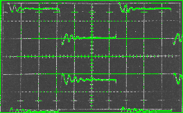 FIGURE 3 6a - Improper Clocks (Note undershoot and overlap)
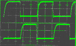 FIGURE 3.6b - Proper Clocks
MCS65O1
Clock Timing Signals
FIGURE 3.6
-141-
FIGURE 3.6b - Proper Clocks
MCS65O1
Clock Timing Signals
FIGURE 3.6
-141-
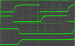 FIGURE 3.7a - Proper Address Lines
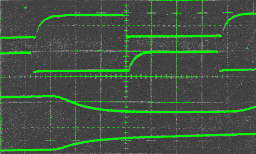 FIGURE 3.7b - Excess Address Line Loading
Address Lines in MCS650X Systems
FIGURE 3.7
-142-
FIGURE 3.7b - Excess Address Line Loading
Address Lines in MCS650X Systems
FIGURE 3.7
-142-
 The Data Bus in MCS650X Systems
FIGURE 3.8
-143-
The Data Bus in MCS650X Systems
FIGURE 3.8
-143-step which will verify the operation of most of the basic system hardware. The tools required are: * Single Cycle/Single Instruction Logic * Oscilloscope * Signal generator (for driving RESET) 3.4.4.1 Static Analysis of System Details Depress the HALT button and then the manual RESET switch; then push the single cycle switch six times. This will step the processor through the first part of the BRK sequence and into the RESET vector fetch. At this time the processor should be generating FFFC on the address bus and the ROM should have put the low order byte of the RESET vector onto the data bus in response to this address. This is an excellent time to check the following very basic items: A. Address Lines: Using the oscilloscope, verify that the logic levels on the address lines are proper and that they are reflected properly through any bus expanders onto the memory and peripheral chips. This is a very important test since improper implemen- tation of bus expanders is a very common circuit fault. B. ROM/PROM chip selects: Using the oscilloscope, verify that the address FFFC does select the ROM which contains the low order byte of the RESET vector. C. Data Bus: Using the oscilloscope, verify that the voltages on the data bus pins of the processor are proper. It is important that these signals be analyzed at the processor to assure proper operation of any bi-directional bus expanders in the system. In this test, the most common indication of improper operation of the data bus expanders is "floating" processor data bus pins, i.e., the processor data bus pins are being driven neither high nor low because the bus expanders are in the open-circuit condition or are reversed.
-144-
D. Miscellaneous Processor Pins: Using the oscilloscope, briefly examine the other processor pins (R/W, IRQ, NMI, etc.) to assure that there are no volt- age level problems detectable at this point. Both of the interrupt inputs and the R/W output should be high. Examine the R/W signal on the input to the memory and peripheral devices. After these initial tests are complete, it should be possible to press the single step switch once more to fetch the high order byte of the interrupt vector from address FFFD. On the next actuation of the single cycle switch, the processor address bus should contain the RESET vector which was fetched from memory. At this point, the processor is ready to execute the system ini- tialization routine. During initialization, it can be expected that pro- gram memory will be accessed, peripheral registers will be loaded, and internal processor registers will be cleared or set to a starting value. It is extremely useful to execute this routine one instruction at a time to determine that each time program memory is accessed, the proper instruction is returned. However, unless a data trap is provided, it will be more meaningful to utilize dynamic analysis techniques to analyze the operation of peripheral devices, since most peripheral accesses will be for the pur- pose of writing either the I/O control or the control registers in the peripheral devices. 3.4.4.2 Dynamic Analysis of System Details The general technique of dynamic analysis is discussed in Section 3.2. The discussion which follows will use this technique to analyze many of the details of the system operation. Set up the system as described in Section 3.2.2. After the test equipment is operating properly, most of the system operation can be veri- fied using only the oscilloscope. 3.4.4.2.1 Address Bus Verification The first item which must be checked is the specific timing of the address lines. These lines will change during the first part of Ø1 but after the specified period, they should stabilize and remain stable through
-145-
the rest of the cycle. Figure 3.7a shows the waveform which one should ex- pect to see while examining Ø1, Ø2 and two address lines. In this illus- tration, one address line is going high and the other is going low. These lines are being generated within the processor and are guaranteed to oper- ate properly provided the total loading on the pins is within specifica- tions. The most common cause of both voltage level and rise time problems is overloading. Voltage level problems are commonly evidenced by the "zero" level being too high, i.e., the address buffer is being asked to sink too much current. Excess capacitance is usually evidenced by the rise atid fall times being too long (Figure 3.7b). In examining the address lines, it is important that the data be examined on the processor and directly on the various support chips. This will assure that any bus expanders in the system are operating properly and that the addresses are valid where they are actually being used. 3.4.4.2.2 Data Bus Verification After the addresses have been verified, the next step is to ex- amine the data bus to verify the validity of data being transferred both from the processor to the support chips and from the support chips back into the processor. Figure 3.8 illustrates the waveform which one can expect to see on the data bus lines. It is very important to note that during Ø1 there is no way to predict the voltage on the data bus since neither the proces- sor nor the support chips are driving these lines. However, during Ø1 the data bus pins should go either high or low. It is only during Ø2 (high) that the validity of the data can be verified. Three very important parameters must be considered when examin- ing the data bus. These are the voltage levels, the time at which the data is valid and the delay from the trailing edge of Ø2 to data becoming in- valid. A. Voltage Levels: The logic levels on the processor data bus must always be greater than 2.4 volts for a logic 1 and less than 0.4 volts for a logic 0. This is a very basic concept but a quick check on these levels very early in the checkout procedure can help the designer avoid hours of attempting to make a
-146-
system operate with signals which are actually marginal but which on the surface appear to be satisfactory. Another very important item to check is whether or not the logic "0" voltage is actually going negative (below GND). It is very important that the logic signals going into all the chip inputs not be allowed to go below -0.3 volts as indicated in the specifications. B. Data Valid Time: The time at which data becomes valid indicates the total time which the processor or memory has available to stabil- ize the gates and latches used to trap the data within the chip. For this reason the data must not take too long to reach either a valid high "1" or a valid low "0." The pri- mary cause of slow signals on the data bus is excessive loading, either resistive or capacitive. Carefully check the devices which are attached to the bus to make sure that the total loading is within specifications. C. Hold Time: The last important consideration, "hold time," is defined as the time between the trailing edge of the Ø2 pulse and the point at which data is no longer valid. A minimum of 10 nsec hold time is required for the processor to trap the data into its internal input latches. The processor inter- nal Ø2 pulse is used to gate the contents of the data bus into these latches. Hold time is also required by the vari- ous support chips within the system. Carefully check the signals as they appear on the RAMs, ROMs, etc. to verify that each is being operated in accordance with its specifi- cation.
-147-
3.4.5 Detailed Component Check After the dynamic check of the reset routine, the next step is to attempt to run the system program. The success of this operation will determine whether or not a further detailed component check is necessary. It is important to note that the checkout of the system program should proceed one step at a time in much the same manner as we have approached the hardware checkout. If a careful examination has been made of all of the devices, data paths, etc. in the system, the software checkout can proceed under the assumption that the hardware is fully operational. How- ever, it is inevitable that doubts will arise. There are times in the software checkout process that the program will appear to be incorrect; data won't be going into memory as it should or, in general, some hardware failure will be indicated. As soon as this happens, the suspected com- ponents should be examined in detail. In keeping with the policy of "one step or one problem at a time," it is important that potential hardware problems not be allowed to invalidate the effort being put into the soft- ware checkout. Component problems can be one of two types: component failure, i.e., a part not operating per specifications; or system failure, i.e., a part being used wrong in the system. The latter problem can be a result of incorrect system design or incorrect wiring. The problem of functional components not operating properly in the system is the one which will be addressed here. In fact, if there is any doubt about a component being functional, it should be replaced immediately upon verification of proper signals to all inputs. If it still does not operate properly, the problem is most likely system related. The detailed component check is performed most effectively by load- ing a small looping program into the system RAM. For this reason, the TIM or KIM debug software (see TIM and KIM Manuals) can be of significant value in this process. The procedure involves static and dynamic operation of a small test program which exercises each of the components in the sys- tem. The goal of this step should be a complete verification that all chip selects are operating properly, that all data address lines are operating properly and that the support chips are driving the processor properly.
-148-
The suggested procedure for checkout of each type of component is discussed separately below. A. ROMs (PROMS): The most straightforward component in any microprocessor system is the ROM. This device simply puts out an 8-bit word onto the data bus in response to an address. Difficulty with ROMS is usually caused by improper chip selects or by mis-application of devices which are not part of the MCS6500 family. For this reason, static testing of ROMs is usually a very effective first step. This requires entering a test program into RAM and exe- cuting this program using the single cycle switch. The program itself should simply perform a READ (for example, an LDA or LDX instruction) of a selected word for each ROM chip to be tested. The chip selects can then be examined and at the same time, the address lines presented to the chips can be examined along with the data put on the data bus. After the chip select, address bus and data bus have been verified statically, it may be necessary to execute the same test program dynamically to assure that all chips in the system are operating at system speed. At this point, it may be neces- sary to include a WRITE operation (STA, STX, STY, etc.) in the loop to provide a sync signal. Analysis of the dynamic operation of the ROMs should involve first looking at each address and data bus lines directly on the processor chip. It is here that the address is being generated, and it is here that the data must meet a speed specification. If data is not valid at the proper time, the next step is to determine where excessive delay has been introduced into the data path from address output, through the ROM and back to the processor data bus. Keep in mind that it is this entire path which must operate at speed to assure proper processor opera- tion. In fact, if the delays are excessive, it may be necessary to slow down the system clock rate to allow the program data to reach the processor in time. An alternative solution to this problem is the implementation of the RDY signal to hold the pro-
-149-
cessor for one cycle each time it fetches data or program from the ROMS. Although the problems discussed above may be encountered at this point, it is much more likely that a wiring error will cause a single address or data line to be excessively loaded so that it operates slow or not at all. This problem can usually be detected and fixed quite easily by looking at each component in the data path. B. RAMs: Operation of the RAMs in a microprocessor system can be checked in much the same manner as the ROMs. Execution of a test loop program both statically and dynamically for each chip in the system should be sufficient to verify proper operation of the RAMs in the system. For each RAM, both a WRITE and a READ oper- ation should be included in the test loop. This will allow checkout of data transfers in both directions. During single cycle execution of the test loop, the proces- sor will stop only in the RAM read operations. However, this will allow a static check of the chip select logic and the address and data lines. Running the program dynamically will allow verification that the data and address signals presented to the RAMs during the WRITE operation are within specifica- tion for the RAM being used in the system and that the total delays through the address, RAM, and data bus path are within specifications for the processor during the READ operations. As with the ROMs, the most likely problem to be encountered at this point is wiring errors which cause a specific device to operate improperly. A careful check of each pin will allow detection of this type of problem. C. PIAs: The peripheral interface devices (6520, 6530, etc.) can all be checked out in the manner described above. However, since these chips do many different operations, the test program must be much more complex than that required for the ROM and RAM.
-150-
However, it can usually be limited to testing only those func- tions which are used in the system. A large part of the operation of the peripheral interface devices can be verified by doing a WRITE followed by a READ for each register on the chip. This will allow a complete checkout of the data paths between the processor and the chips as well as a checkout of all the chip select functions. However, a more complete analysis may be required to verify that data is appear- ing properly on the output pins of the peripheral chip and that data on the inputs is being reflected properly back into the processor. This will involve disconnecting the peripheral sub- system which the processor is attempting to drive and manually putting data into the inputs. A separate test can verify the validity of output data. After the system hardware has been examined in the detail discussed above, the designer will have developed confidence that his system can operate properly once the system program is completely debugged. Verification of the system pro- gram should proceed with a section-by-section checkout as discussed above. Each subroutine, interrupt routine, etc. should be examined separately. They can then be combined to form the major peripheral operating routines, arithmetic routines, etc. that make up the system. The final result should be a function- ing program which has been examined in all its details running on a system which is fully operational.
-151-
APPENDIX A SUMMARY OF SINGLE CYCLE EXECUTION
This section contains an outline of the data on both the address bus and the data bus for each cycle of the various processor instructions. It tells the system designer exactly what to expect while single cycling through a program. Note that the processor will not stop in any cycle where R/W is a 0 (write cycle). Instead, it will go right into the next read cycle and stop there. For this reason, some instructions may appear to be shorter than indicated here. All instructions begin with T0 and the fetch of the OP CODE and continue through the required number of cycles until the next T0 and the fetch of the next OP CODE. While the basic terminology used in this appendix is discussed in the Pro- gramming Manual, it has been defined below for ease of reference while studying Single Cycle Execution. OP CODE--The first byte of the instruction containing the operator and mode of address. OPERAND--The data on which the operation specified in the OP CODE is performed. BASE ADDRESS--The address in Indexed addressing modes which specifies the loca- tion in memory to which indexing is referenced. The high order of byte of the base address (AB08 to AB15) is BAH (Base Address High) and the low order byte of the base address (AB00 to AB07) is BAL (Base Address Low). EFFECTIVE ADDRESS--The destination in memory in which data is to be found. The effective address may be loaded directly as in the case of Page Zero and Absolute Addressing or may be calculated as in Indexing operations. The high order byte of the effective address (AB08 to AB15) is ADH and the low order byte of the effective address (AB00 to AB07) is ADL. INDIRECT ADDRESS--The address found in the operand of instructions utilizing (Indirect),Y which contains the low order byte of the base address. IAH and IAL represent the high and low order bytes. JUMP ADDRESS--The value to be loaded into Program Counter as a result of a Jump instruction.A-1
A. 1. SINGLE BYTE INSTRUCTIONS ASL DEX NOP TAX TYA CLC DEY ROL TAY CLD INX SEC TSX CLI INY SED TXA CLV LSR SEI TXS These single byte instructions require two cycles to execute. During the second cycle the address of the next instruction in program sequence will be placed on the address bus. However, the OP CODE which appears on the data bus during the second cycle will be ignored. This same instruction will be fetched on the following cycle at which time it will be decoded and executed. The ASL, ROL and LSR instructions apply to the accumulator mode of address. Tn Address Bus Data Bus R/W Comments T0 PC OP CODE 1 Fetch OP CODE T1 PC + 1 OP CODE 1 (Discarded) T0 PC + 1 OP CODE 1 Next Instruction A. 2. INTERNAL EXECUTION ON MEMORY DATA ADC CMP EOR LDY AND CPX LDA ORA BIT CPY LDX SBC The instructions listed above will execute by performing operations in- side the microprocessor using data fetched from the effective address. This total operation requires three steps. The first step (one cycle) is the OP CODE fetch. The second (zero to four cycles) is the calculation of an effective address. The final step is the fetching of the data from the effective address. Execution of the instruction takes place during the fetching and decoding of the next instruction.
A-2
A. 2.1. Immediate Addressing (2 cycles) Tn Address Bus Data Bus R/W Comments T0 PC OP CODE 1 Fetch OP CODE T1 PC + 1 Data 1 Fetch Data T0 PC + 2 OP CODE 1 Next Instruction A. 2.2. Zero Page Addressing (3 cycles) Tn Address Bus Data Bus R/W Comments T0 PC OP CODE 1 Fetch OP CODE T1 PC + 1 ADL 1 Fetch Effective Address T2 00, ADL Data 1 Fetch Data T0 PC + 2 OP CODE 1 Next Instruction A. 2.3. Absolute Addressing (4 cycles) Tn Address Bus Data Bus R/W Comments T0 PC OP CODE 1 Fetch OP CODE T1 PC + 1 ADL 1 Fetch low order Effective Address byte T2 PC + 2 ADH 1 Fetch high order Effective Address byte T3 ADH, ADL Data 1 Fetch Data T0 PC + 3 OP CODE 1 Next Instruction A. 2.4. Indirect, X Addressing (6 cycles) Tn Address Bus Data Bus R/W Comments T0 PC OP CODE 1 Fetch OP CODE T1 PC + 1 BA1 1 Fetch Page Zero Base Address T2 00, BAL Data 1 (Discarded) T3 00, BAL + X ADL 1 Fetch low order byte of Effective Address T4 00, BAL + ADH 1 Fetch high order byte of X + L Effective Address T5 ADH, ADL Data 1 Fetch Data T0 PC + 2 OP CODE 1 Next Instruction
A-3
A. 2.5. Absolute, X or Absolute, Y Addressing (4 or 5 cycles) Tn Address Bus Data Bus R/W Comments T0 PC OP CODE 1 Fetch OP CODE T1 PC + 1 BAL 1 Fetch low order byte of Base Address T2 PC + 2 BAH 1 Fetch high order byte of Base Address T3 ADL: BAL + Data* 1 Fetch data (no page cross- index register ing) ADH: BAH + C Carry is 0 or 1 as re quired from previous add operation T4* ADL: BAL + Data 1 Fetch data from next page index register ADH: BAH + 1 T0 PC + 3 OP CODE 1 Next Instruction *If the page boundary is crossed in the indexing operation, the data fetched in T3 is ignored. If page boundary is not crossed, the T4 cycle is bypassed. A. 2.6. Zero Page, X or Zero Page, Y Addressing Modes (4 cycles) Tn Address Bus Data Bus R/W Comments T0 PC OP CODE 1 Fetch OP CODE T1 PC + 1 BAL 1 Fetch Page Zero Base Address T2 00, BAL Data 1 (Discarded) T3 00, BAL + Data 1 Fetch Data (no page cross index ing) register T0 PC + 2 OP CODE 1 Next Instruction
A-4
A. 2.7. Indirect, Y Addressing Hode (5 or 6 cycles) Tn Address Bus Data Bus R/W Comments T0 PC OP CODE 1 Fetch OP CODE T1 PC + 1 IAL 1 Fetch Page Zero Indirect Address T2 00, IAL BAL 1 Fetch low order byte of Base Address T3 00, IAL + 1 BAH 1 Fetch high order byte of Base Address T4 ADL: BAL + Y Data* 1 Fetch Data from same page ADH: BAH + C Carry is 0 or 1 as re quired from previous add operation T5* ADL: BAL + Y Data 1 Fetch Data from next page ADH: BAH + 1 T0 PC + 2 OP CODE 1 Next Instruction *If page boundary is crossed in indexing operation, the data fetch in T4 is ignored. If page boundary is not crossed, the T5 cycle is by- passed. A. 3. ST0RE OPERATIONS STA STX STY The specific steps taken in the Store Operations are very similar to those taken in the previous group (Internal execution on memory data). However, in the Store Operation, the fetch of data is replaced by a WRITE (R/W = 0) cycle. No overlapping occurs and no shortening of the instruction time occurs on indexing operations. A. 3.1. Zero Page Addressing (3 cycles) Tn Address Bus Data Bus R/W Comments T0 PC OP CODE 1 Fetch OP CODE T1 PC + 1 ADL 1 Fetch Zero Page Effective Address T2 00, ADL Data 0 Write internal register to memory T0 PC + 2 OP CODE 1 Next Instruction
A-5
A. 3.2. Absolute Addressing (4 cycles) Tn Address Bus Data Bus R/W Comments T0 PC OP CODE 1 Fetch OP CODE T1 PC + 1 ADL 1 Fetch low order byte of Effective A0dress T2 PC + 2 ADH 1 Fetch high order byte of Effective Address T3 ADH, ADL Data 0 Write internal register to memory T0 PC + 3 OP CODE 1 Next Instruction A. 3.3. Indirect, X Addressing (6 cycles) Tn Address Bus Data Bus R/W Comments T0 PC OP CODE 1 Fetch OP CODE T1 PC + 1 BAL 1 Fetch Page Zero Base Address T2 00, BAL Data 1 (Discarded) T3 00, BAL + X ADL 1 Fetch low order byte of Effective Address T4 00, BAL + ADH 1 Fetch high order byte of X + 1 Effective Address T5 ADH, All Data 0 Write internal register to memory T0 PC + 2 OP CODE 1 Next Instruction A. 3.4. Absolute, X or Absolute, Y Addressing (5 cycles) Tn Address Bus Data Bus R/W Comments T0 PC OP CODE 1 Fetch OP CODE T1 PC + 1 BAL 1 Fetch low order byte of Base Address T2 PC + 2 BAH 1 Fetch high order byte of Base Address T3 ADL: BAL + Data 1 index (Discarded) register ADH: BAH + C T4 ADH, ADL Data 0 Write internal register to memory T0 PC + 3 OP CODE 1 Next Instruction
A-6
A. 3.5. Zero Page, X or Zero Page, Y Addressing Modes (4 cycles) Tn Address Bus Data Bus R/W Comments T0 PC OP CODE 1 Fetch OP CODE T1 PC + 1 BAL 1 Fetch Page Zero Base Address T2 00, BAL Data 1 (Discarded) T3 ADL: BAL + Data 0 Write internal register index to memory register T0 PC + 2 OP CODE 1 Next Instruction A. 3.6. Indirect, Y Addressing Mode (6 cycles) Tn Address Bus Data Bus R/W Comments T0 PC OP CODE 1 Fetch OP CODE T1 PC + 1 IAL 1 Fetch Page Zero Indirect Address T2 00, IAL BAL 1 Fetch low order byte of Base Address T3 00, IAL + 1 BAH 1 Fetch high order byte of Base Address T4 ADL: BAL + Y Data 1 (Discarded) ADH: BAH T5 ALH, ADI Data 0 Write Internal Register to memory T0 PC + 2 OP CODE 1 Next Instruction A. 4. READ--MODIFY--WRITE OPERATIONS ASL LSR DEC ROL INC ROR The Read--Modify--Write operations involve the loading of operands from the operand address, modification of the operand and the resulting modi- fied data being stored in the original location. Note: The ROR instruction will be available on MCS650X microprocessors after June, 1976.
A-7
A. 4.1. Zero Page Addressing (5 cycles) Tn Address Bus Data Bus R/W Comments T0 PC OP CODE 1 Fetch OP CODE T1 PC + 1 All 1 Fetch Page Zero Effective Address T2 00, ADL Data 1 Fetch Data T3 00, ADL Data 0 T4 00, ADL Modified 0 Write modified Data back Data to memory T0 PC + 2 OP CODE 1 Next Instruction A. 4.2. Absolute Addressing (6 cycles) Tn Address Bus Data Bus R/W Comments T0 PC OP CODE 1 Fetch OP CODE T1 PC + 1 ADL 1 Fetch low order byte of Effective Address T2 PC + 2 ADH 1 Fetch high order byte of Effective Address T3 ADH, ADL Data 1 T4 ADH, ADL Data 0 T5 ADH, ADL Modified 0 Write modified Data back Data into memory T0 PC + 3 OP CODE 1 Next Instruction A. 4.3. Zero Page, X Addressing (6 cycles) Tn Address Bus Data Bus R/W Comments T0 PC OP CODE 1 Fetch OP CODE T1 PC + 1 BAL 1 Fetch Page Zero Base Address T2 00, BAL Data 1 (Discarded T3 ADL: BAL + X Data 1 Fetch Data (without carry) T4 ADL: BAL + X Data 0 (without carry) T5 ADL: BAL + X Modified 0 Write modified Data back (without Data into memory carry) T0 PC + 2 OP CODE 1 Next Instruction
A-8
A. 4.4. Absolute, X Addressing (7 cycles) Tn Address Bus Data Bus R/W Comments T0 PC OP CODE 1 Fetch OP CODE T1 PC + 1 BAL 1 Fetch low order byte of Base Address T2 PC + 2 BAH 1 Fetch high order byte of Base Address T3 ADL: BAL + X Data 1 (Discarded) ADH: BAH + C T4 ADL: BAL + X Data 1 Fetch Data ADH: BAH + C T5 ADH, ADL Data 0 T6 ALH, ADL Modified 0 Write modified Data back Data into memory T0 PC + 3 OP CODE 1 New Instruction A. 5. MISCELLANEOUS OPERATIONS BCC BRK PHP BCS BVC PLA BEQ BVS PLP BMI JMP RTI BNE JSR RTS BPL PHA A. 5.1. Push Operation--PHP, PHA (3 cycles) Tn Address Bus Data Bus R/W Comments T0 PC OP CODE 1 Fetch OP CODE T1 PC + 1 OP CODE 1 Discarded) T2 Stack Pointer* Data 0 Write Internal Register into Stack T0 PC + 1 OP CODE 1 Next Instruction *Subsequently referred to as "Stack Ptr."
A-9
A. 5.2. Pull Operations--PLP, PLA (4 cycles) Tn Address Bus Data Bus R/W Comments T0 PC OP CODE 1 Fetch OP CODE T1 PC + 1 OP CODE 1 (Discarded) T2 Stack Ptr. Data 1 (Discarded) T3 Stack Ptr. + 1 Data 1 Fetch Data from Stack T0 PC + 1 OP CODE 1 Next Instruction A. 5.3. Jump to Subroutine--JSR (6 cycles) Tn Address Bus Data Bus R/W Comments T0 PC OP CODE 1 Fetch OP CODE T1 PC + 1 ADL 1 Fetch low order byte of Subroutine Address T2 Stack Ptr. Data 1 (Discarded) T3 Stack Ptr. PCH 0 Push high order byte of program counter to Stack T4 Stack Ptr. - 1 PCL 0 Push low order byte of program counter to Stack T5 PC + 2 ADH 1 Fetch high order byte of Subroutine Address T0 Subroutine OP CODE 1 Next Instruction Address (ADH, ADL)
A-10
A. 5.4. Break Operation--(Hardware Interrupt)-BRK (7 cycles) Tn Address Bus Data Bus R/W Comments T0 PC OP CODE 1 Fetch ERK OP CODE (or force BRK) T1 PC + 1 Data 1 (PC on hard- (Discarded) ware inter rupt) T2 Stack Ptr. PCH 0 Push high order byte of program counter to Stack T3 Stack Ptr. - 1 PCL 0 Push low order byte of program counter to Stack T4 Stack Ptr. - 2 P 0 Push Status Register to Stack T5 FFFE ADL 1 Fetch low order byte of (NMI-FFFA) interrupt vector (RES-FFFC) T6 FFFF ADH 1 Fetch high order byte of (NNI-FFFB) interrupt vector (RES-FFFD) T0 Interrupt Vec- OP CODE 1 Next Instruction tor (ADH, ADL) A. 5.5. Return from Interrupt-RTI (6 cycles) Tn Address Bus Data Bus R/W Comments T0 PC OP CODE 1 Fetch OP CODE T1 PC + 1 Data 1 (Discarded) T2 Stack Ptr. Data 1 (Discarded) T3 Stack Ptr. + 1 Data 1 Pull P from Stack T4 Stack Ptr. + 2 Data 1 Pull PCL from Stack T5 Stack Ptr. + 3 Data 1 Pull PCH from Stack T0 PCH, PCL OP CODE 1 Next Instruction
A-11
A. 5.6. Jump Operation--JMP A.5.6.l.Absolute Addressing Mode (3 cycles) Tn Address Bus Data Bus R/W Comments T0 PC OP CODE 1 Fetch OP CODE T1 PC + 1 ADL 1 Fetch low order byte of Jump Address T2 PC + 2 ADH 1 Fetch high order byte of Jump Address T0 ADH, ADL OP CODE 1 Next Instruction A.5.6.2.Indirect Addressing Mode (5 cycles) Tn Address Bus Data Bus R/W Comments T0 PC OP CODE 1 Fetch OP CODE T1 PC + 1 IAL 1 Fetch low order byte of Indirect Address T2 PC + 2 IAH 1 Fetch high order byte of Indirect Address T3 IAH, IAL ADL 1 Fetch low order byte of Jump Address T4 IAH, IAL + 1 ADH 1 Fetch high order byte of Jump Address T0 ADH, ADL OP CODE 1 Next Instruction A. 5.7. Return from Subroutine--RTS (6 cycles) Tn Address Bus Data Bus R/W Comments T0 PC OP CODE 1 Fetch OP CODE T1 PC + 1 Data 1 (Discarded) T2 Stack Ptr. Data 1 (Discarded) T3 Stack Ptr. + 1 PCL 1 Pull PCL from Stack T4 Stack Ptr. + 2 PCH 1 Pull PCH from Stack T5 PCH, PCL (from Data 1 Stack) (Discarded) T0 PCH, PCL + 1 OP CODE 1 Next Instruction
A-12
A. 5.8. Branch Operation--BCC, BCS9 BEQ, BMI, BNE, BPL, BVC9 BVS (2, 3, or 4 cycles) Tn Address Bus Data Bus R/W Comments T0 PC OP CODE 1 Fetch OP CODE T1 PC + 1 Offset 1 Fetch Branch Offset T2* PC + 2 + OP CODE 1 Offset Added to Program offset (w/o Counter carry) T3** PC + 2 + OP CODE 1 Carry Added offset (with carry) *Skip if branch not taken **Skip if branch not taken; skip if branch operation doesn t cross page boundary
A-13